Semiconductor Lithography Systems
Successfully developing smaller and more functional semiconductors while contributing to the digital evolution of society
A wide range of products such as smartphones and electrical appliances are becoming smaller and more functional, and all are now part of everyday life.
Semiconductor lithography technology from Nikon is making a significant contribution to the evolution of semiconductors (semiconductor integrated circuits), which are indispensable components of these products.
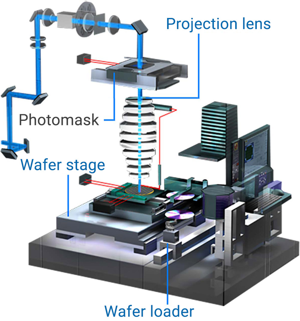
A semiconductor lithography system undertakes a process whereby highly complex circuit patterns drawn on a photomask made of a large glass plate are reduced using ultra-high-performance lenses and exposed onto a silicon substrate known as a wafer.
Semiconductor lithography systems require three key technologies and these determine their performance.
The first technology is "the resolution capability of the projection lens." The better the resolving power of the lens, the more intricate a circuit pattern can be when it is optically transferred. To improve lens performance, Nikon manages quality through an integrated system of production from the blending of raw materials for the lens to dissolving, grinding, coating, and assembly.
The second technology is "alignment accuracy." To produce a single semiconductor, photomasks must be replaced tens of times and circuit patterns must be repeatedly etched in the exposure process. It is therefore of critical importance that the silicon wafer and photomask are perfectly aligned each time. Nikon uses multiple sensors to accurately position the photomask and silicon wafer.
The third vital component is "throughput." This technology is important when semiconductors are mass-produced. Throughput is an indication of productivity, which is expressed by the number of silicon wafers that can be exposed in an hour. To expose the maximum number of semiconductors on a single wafer and boost throughput, Nikon has developed the ability to move the stage that holds the wafer in position at extremely high speeds.
By combining these three technologies, Nikon has succeeded in making semiconductor lithography systems that are described as "the most precise machines in history."
Immersion lithography

Since their advent, semiconductors have rapidly become smaller and an increasing number of functions can be achieved with them. As this evolution has progressed, Nikon has continued to develop lithography technologies with higher resolution capabilities to keep up with the ongoing miniaturization of semiconductors. With the progress of miniaturization, however, a theoretical barrier was reached that prevented existing lithography technology from handling the smaller sizes. The solution to this problem was immersion lithography technology, which Nikon incorporated into its semiconductor lithography systems.
Immersion lithography achieves a higher resolving power by filling the space between the projection lens and the wafer with purified water — the refractive index of purified water is higher at 1.44 than that of air (1.00). In immersion lithography, purified water itself is used like a lens.
This technology makes it possible to overcome the aforementioned barrier and fabricate semiconductors that are smaller than 40 nanometers in size.
Multiple patterning
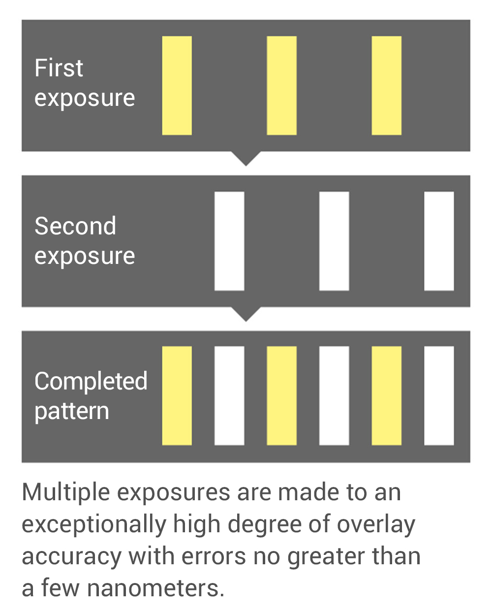
Along with immersion lithography, another technique that supports the latest semiconductor manufacturing is multiple patterning. Multiple patterning refers to a circuit pattern that has been divided into two or more patterns with a feature density low enough to be printed with an existing semiconductor lithography system, which are then combined to ultimately render a high feature density.
This process may seem simple when described in theoretical terms. In the actual semiconductor production process, however, multiple circuit pattern layers are built up through iterations of exposure onto the same wafer with extremely high overlay accuracy, keeping the shift of the exposure positions minimal.
Achieving the extremely high overlay accuracy required, allowing errors no greater than a few nanometers, with a high level of productivity at the same time, mass production of devices with 20 nm nodes or smaller was effectively attained.
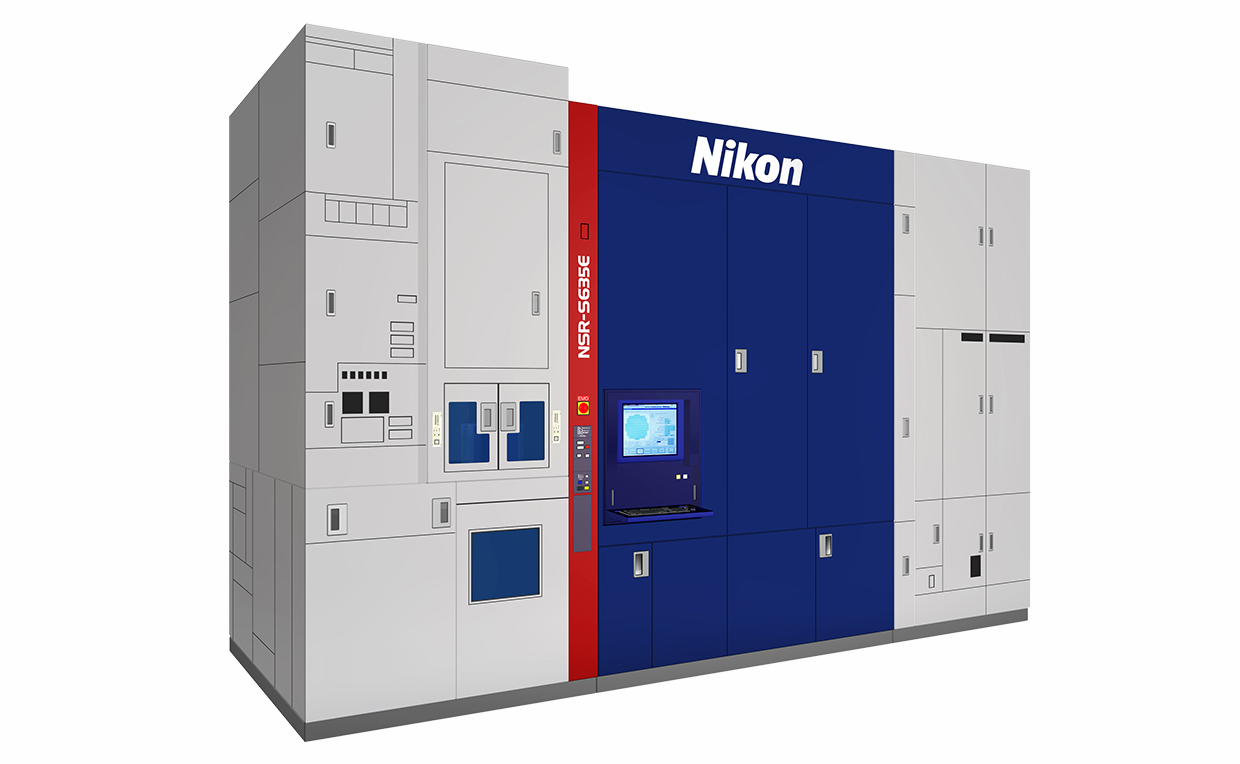
The NSR-S635E ArF Immersion Scanner, developed for use in 5nm node processes for high-volume semiconductor manufacturing, realized mix-and-match overlay (MMO*) of 2.1 nm or below and productivity delivering throughput capabilities of over 275 wafers per hour.
- *Mix-and-Match Overlay (MMO) refers to overlay accuracy among multiple identical scanners.
Product Technology
- Digital SLR cameras
- Mirrorless cameras
- Binoculars
- FPD Lithography Systems
- Semiconductor Lithography Systems
- Alignment Station
- Super Resolution Microscopes
- Ultra-Wide Field Retinal Imaging Device
- Video Measuring Systems
- Industrial X-ray/CT Inspection Systems
- Non-Contact Large-Volume Inspection System