Business
Whether in manufacturing, advanced medicine, or R&D, Nikon products and solutions will support you in a wide range of situations.

- IC Chips / Electronics
- Machinery / Heavy Industry / Construction
- Biotechnology / Medical
- Automotive / Aviation / Space Exploration
- Resources / Energy / Materials
Covering lithography systems for producing semiconductors and high-definition FPDs, as well as measuring systems for a variety of electronic components. Also includes various optical glass and optical materials.
Device Production
-
FPD Lithography Systems
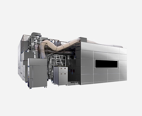
For producing panels employed by large-sized TVs and high-definition smart devices
-
Semiconductor Lithography Systems
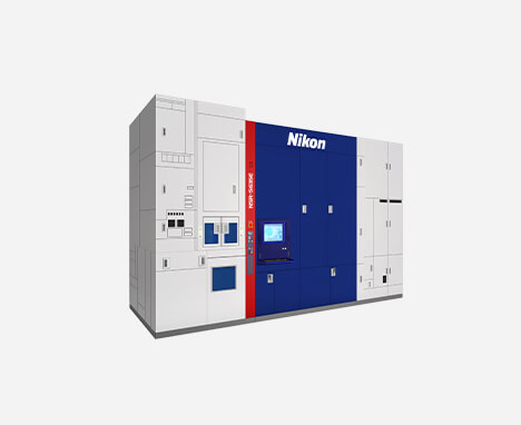
For producing semiconductors employed by cutting-edge processors/memories
Measurement / Inspection / Analysis
-
Alignment Station "Litho Booster"
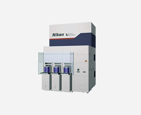
Realizes high-speed, highly accurate wafer measurement for greatly improved lithography accuracy
-
Optical Manual Measuring

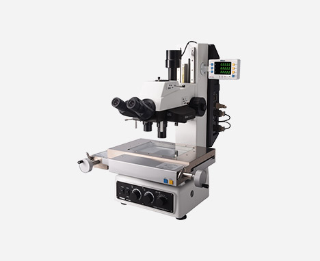
For measuring sizes/shapes of precision parts
-
Video Measuring Systems
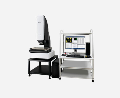
Automated video measurement of sizes/shapes of precision parts
-
X-Ray and CT Systems
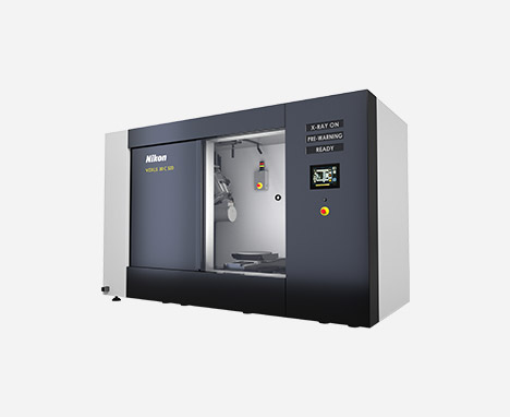
For measuring internal/external dimensions without disassembling the product
-
Industrial Microscopy
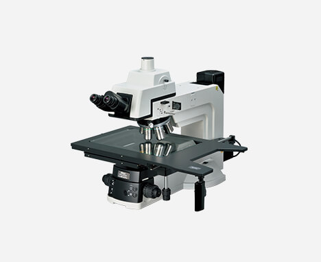
Versatile observation with high optical performance
-
Metrology/Inspection Systems
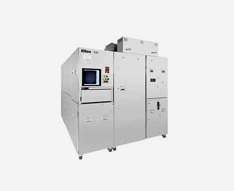
Automatic macro/exterior inspection of IC wafers, Illumination for Imaging Sensor Inspection
-
Digital Micrometer System "Digimicro"
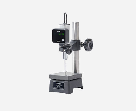
Indication of thickness/differences of parts in units of 0.01µm
Metal Processing
-
Metal AM 3D Printer (DED)
From additive manufacturing as a 3D printer, to laser marking and welding
-
Metal AM 3D Printer (L-PBF)
Offering a lineup of innovative metal 3D printers using cutting-edge L-PBF (Laser-Powder Bed Fusion) technology.
-
Precision Subtractive Processing
Enabling highly precise and complicated processing with ultra-short pulse laser and on-machine measurement.
-
Material Processing Solutions
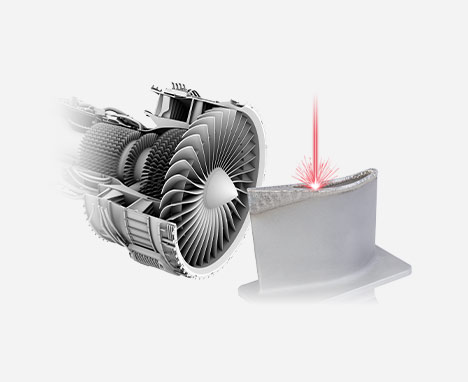
Offering various solutions for metal processing, precision subtractive processing, and riblet processing
Robot Control
-
Robot Vision
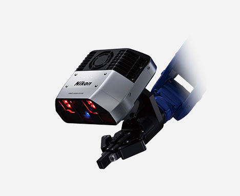
High-speed sensing for 2D/3D cameras and hand vision
Parts / Units
-
Industrial Lenses
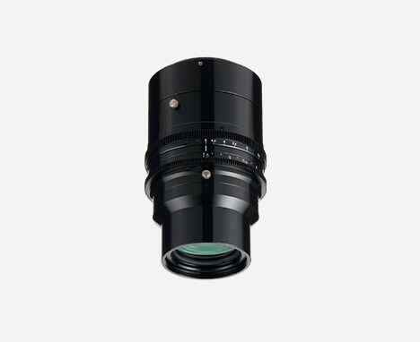
Compatible with high-resolution, large line-sensor cameras
-
Absolute Encoders
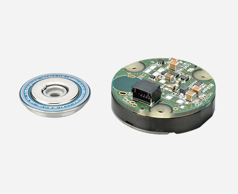
Sensors capable of detecting absolute rotational displacement values
-
Intelligent Actuator Units
Combining a motor, speed reducer, motor driver, brake and encoders. Utilizing multiple intelligent actuator units together facilitates easier building of robots.
-
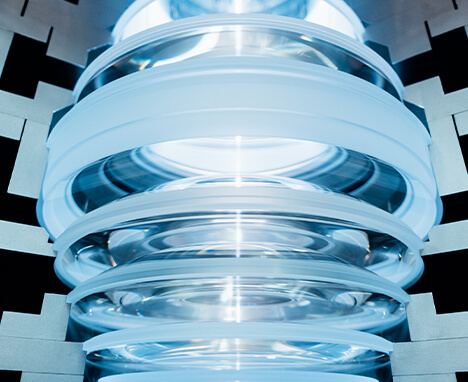
Optical Glass
Optical glass delivering high transparency and superior homogeneity
-
Optical Components & Materials
Optical components (light source, projection lens, etc.) and materials (synthetic silica glass, calcium fluoride, etc.)
Can't find your product and service information?
You can also view information on products and services from each country and region via the link below.
Inquiries about products and services
News
-
Dec. 11, 2025
-
Dec. 10, 2025
-
Nov. 26, 2025
-
Oct. 23, 2025
-
Sep. 25, 2025
Featured
Smart Imaging System "ECLIPSE Ji"
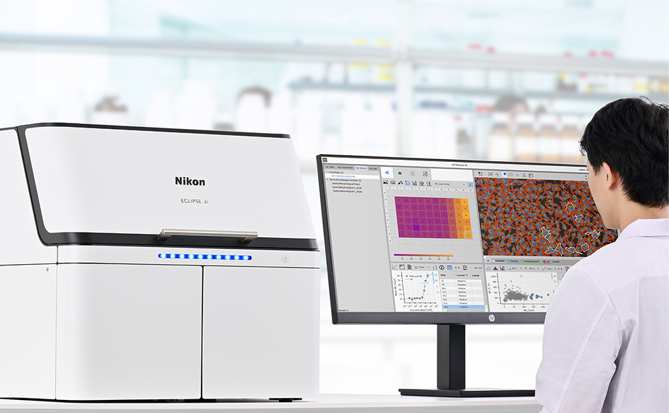
Utilizing AI to accelerate research and development for drug discovery and biological studies.
AX / AX R Confocal Microscope System
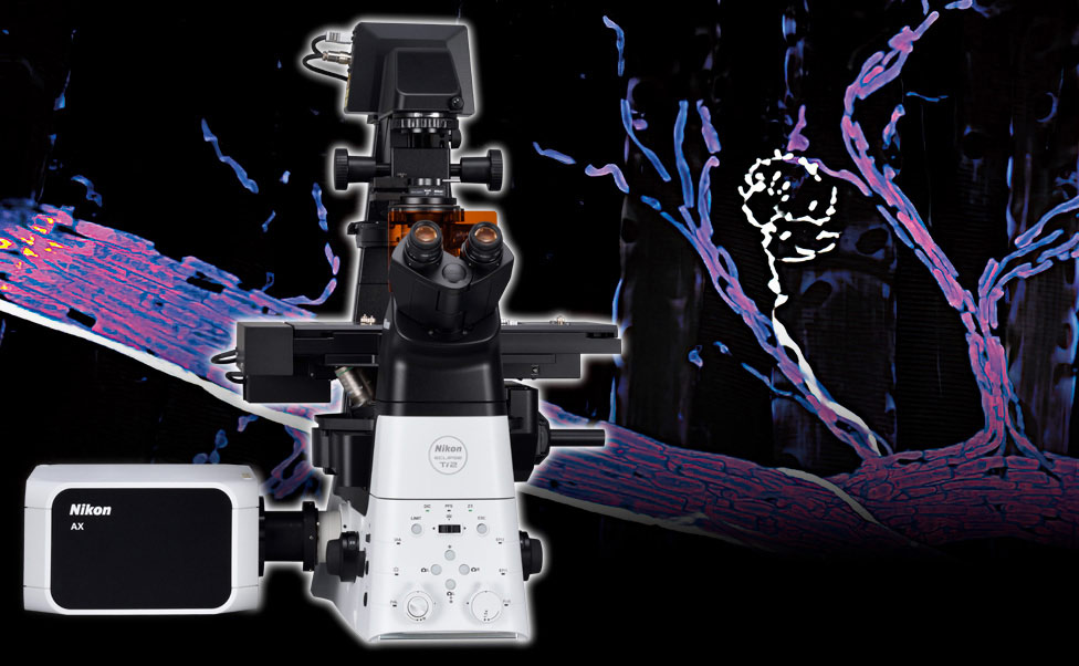
High resolution 8K x 8K images and the world's largest FOV of 25 mm enable you to obtain more data than ever, expanding the possibilities of a wide range of research fields.
Nikon's Contract Research Service (Nikon BioImaging Lab)
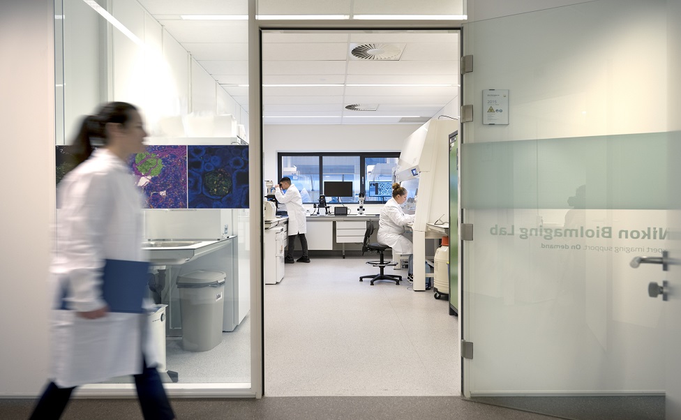
Nikon BioImaging lab is a global Contract Research Organization with a focus on microscopic imaging services. We provide high-resolution imaging solutions and analysis to deal with even difficult-to-image samples, including organoids and micro physiological systems (MPS).
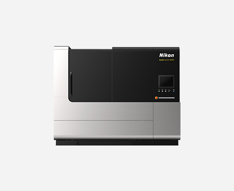
Material Processing Solutions
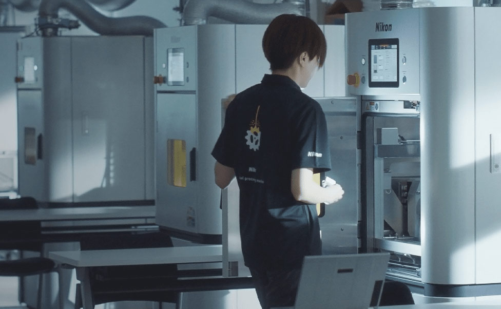
We provide material processing solutions that utilize Nikon's technologies, such as additive manufacturing using metal 3D printers, precision subtractive processing and riblet processing using laser processing machines.
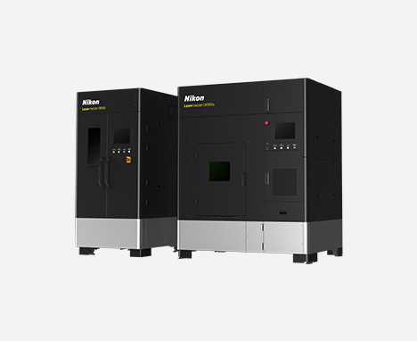
Lasermeister Series
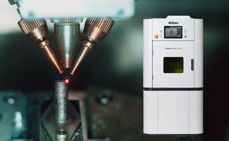
More convenient and easier metal modeling. Additive manufacturing with built-in measurement system.
NSR-2205iL1 5x Reduction i-line Stepper
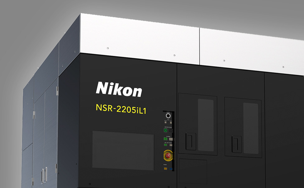
The NSR-2205iL1 is an i-line stepper that will be utilized to manufacture a wide range of devices. It provides excellent affordability and will enable optimized production of various semiconductor devices regardless of the wafer material.