Launch of “S3S LAB”, a Co-Creation Platform Equipped with Roll-to-Roll Maskless Lithography System
Accelerating the Commercialization of Flexible Electronics
December 10, 2025
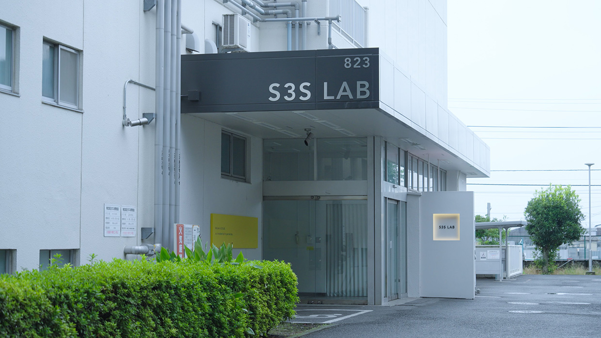
TOKYO - Nikon Corporation will open and commence operation of “S3S LAB”, a co-creation platform outfitted with a full suite of equipment necessary for developing flexible electronics within its Sagamihara Plant in Kanagawa prefecture on December 10, 2025. “S3S LAB” will house Nikon's proprietary, cutting-edge Roll-to-Roll (R2R)*1 maskless lithography system, as well as peripheral equipment utilizing the film deposition and multilayer wiring formation technologies required for flexible device manufacturing. As a new base for innovation, it will provide strong solutions to customers' challenges, from research and development to commercialization.
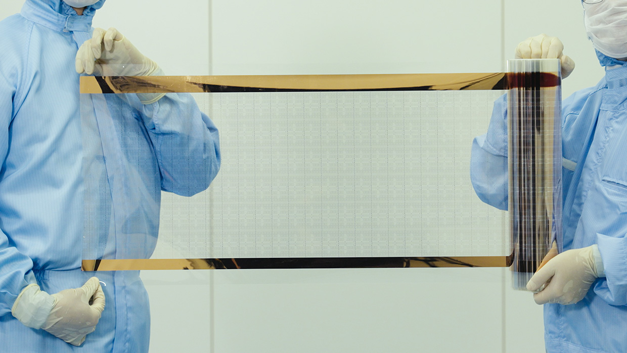
Flexible electronics, which form electronic circuits on the surface of film, enables production of lightweight, thin, transparent, and freely shaped devices. This opens up new possibilities in a variety of fields, including displays, sensors, and perovskite solar cells. However, the transition from research and development to mass production poses the challenge of expensive capital investment and co-creation platforms that can consistently verify the R2R process are rare even on a global scale.
“S3S LAB” provides integrated support from prototype manufacturing to mass production process development, enabling customers to promote necessary process verifications for mass production, and commercialization decisions without large-scale capital investment. In the mass production phase, Nikon will contribute to customers' commercialization and the creation of a new era in the flexible electronics industry by providing process technology and R2R equipment cultivated at “S3S LAB”.
- *1A manufacturing process in which roll-shaped substrates are continuously processed and rewound into rolls. Compared to the sheet processing method, it features superior continuity and high productivity.
Overview of S3S LAB
| Location | 10-1, Asamizodai 1-chome, Minami-ku, Sagamihara, Kanagawa, Japan (within Nikon Sagamihara Plant) |
|---|---|
| Main Services | ・Prototype manufacturing ・Providing total solutions including mass production process development |
| Operation Start Date | December 10, 2025 |
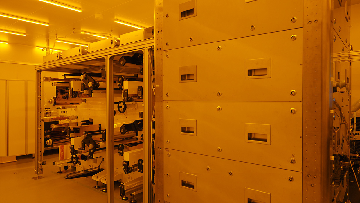
| Main Equipment | R2R Maskless Lithography System, Cleaning System, Slit Die Coating System, HMDS Coating System, Thermal Annealing System, Developing System, Etching System, Peeling System, Optical Inspection System, laminating System, CVD/RIE System, Vacuum Sputtering System, Mist Coating System, Vacuum Vapor Deposition System |
| Usage | Advance reservations required |
Features of the R2R Maskless Lithography System
- Achieves 6.0 µm*2 (L/S*3) resolution and overlay accuracy within ± 2 µm for films prone to deformation such as distortion and shrinkage due to heat, supporting the production of high-definition and multilayer wiring devices.
- Delivers high productivity of 10 mm per second by utilizing multi-lens technology*4 developed with Nikon's FPD lithography systems.
- The polygon scanning method is used to pattern on the curved surface of the roll, enabling continuous patterning.
- Since exposure is based on CAD data, no photomask is required, which contributes to shortening prototyping time and reducing mask costs.
- *21 µm (micrometer) means one-millionth of a meter (one-thousandth of a millimeter).
- *3Abbreviation for Line and Space. Refers to the width of the wiring and the spacing between adjacent wiring.
- *4Nikon's proprietary technology for FPD lithography systems arranges multiple projection lenses in an array and precisely controls them to achieve the same effect as using a single giant lens. This enables patterning over a wider area in a single scan.
Overview of the R2R Maskless Lithography System
![]() Swipe horizontally to view full table.
Swipe horizontally to view full table.
| Product Name | Roll to Roll Maskless Lithography System |
|---|---|
| Resolution | 6.0 µm L/S |
| Light Source | i-line equivalent |
| Overlay Accuracy | ≦± 2 µm |
| Supported Film Width | 400 mm or less (other sizes available upon request) |
| Throughput | 10 mm/sec (Dose: 100 mJ/cm2, resist film thickness: 1.4 µm) |
For details on the R2R maskless Lithography system, please refer to the Nikon Research Report below.
The information is current as of the date of publication. It is subject to change without notice.