| 1910s |
- The Optics Division of Tokyo Keiki Manufacturing and the Mirror Division of Iwaki Glass Manufacturing merge to form Nippon Kogaku Kogyo K.K. (Japan Optical Industries Corp.) using capital provided by Koyata Iwasaki, president of Mitsubishi (1917).
- Oi Plant is completed (1918).
- Optical glass manufacturing research is launched (1918).
|
| 1920s |
- Eight German specialists are invited to Nikon to provide technical instruction (1921).
|
| 1940s |
- Nikon is listed on both the Tokyo and Osaka stock exchanges (1949).
|
| 1960s |
- Oi Plant's Ofuna site (now Yokohama Plant) is built (1967).
- K.K. Tachibana Seisakusho (corporate name changed to Mito Nikon Corporation in 1977, Mito Nikon Precision Corporation in 2007, dissolved in 2010) is established (1968).
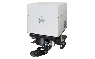
- Ruling Engine No. 1 is installed at Tokyo University of Education (1964).
|
| 1970s |
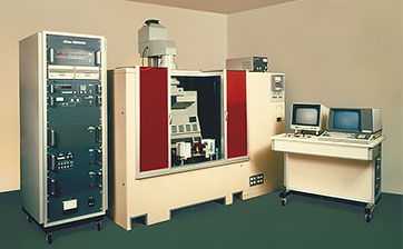
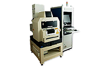
- Development of the SR-1 machine begins (commission from VLSI Technology Research Association) (1976).
- SR-1 machine is completed (1978).
- Nikko Engineering Co., Ltd. (now Nikon Engineering Co., Ltd.) is established (1978).
|
| 1980 |
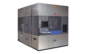
- Announces and starts shipment of NSR-1010G (resolution: 1.0 µm (1,000 nm)), first stepper produced in Japan
|
| 1981 |
- Zao Nikon Co., Ltd. (now Miyagi Nikon Precision Co., Ltd.) is established.
- NSR-1505G (resolution: 1,200 nm)
|
| 1982 |
- Nikon Precision Inc. (abbreviated NPI) is established in the U.S.
- A specialized plant for lithography system VLSI manufacturing systems is completed within the Yokohama Plant.
- First shipment of lithography systems to the U.S.
- OPTISTATION IC wafer inspection system
|
| 1983 |
- Production space is expanded for specialized stepper plant within the Yokohama Plant.
|
| 1984 |
- Kumagaya Plant is built.
- NSR-1505G2A (resolution: 1,000 nm)
- NSR-1010i2 (resolution: 800 nm), first i-line stepper produced in the world
|
| 1985 |
- NSR-HT3025G (resolution: 2,000 nm)
|
| 1987 |
- Nikon Tec Corporation is established.
- NSR-1505G4B (resolution: 900 nm)
- SX-5 (resolution: 500 nm)
- Number of semiconductor lithography systems sold reaches 1,000.
|
| 1988 |
- Corporate name is changed to Nikon Corporation.
- Nikon Precision Europe GmbH (abbreviated NPE) is established in West Germany.
- NSR-1505EX (resolution: 500 nm), first excimer stepper produced in the world
- NSR-1505G6E (resolution: 650 nm)
|
| 1989 |
- Second stage of Kumagaya Plant construction is completed.
- NSR-1505i6A (resolution: 650 nm)
- Number of semiconductor lithography systems sold reaches 2,000.
- NSR-1755G7A (resolution: 650 nm)
|
| 1990 |
- Nikon Precision Korea Ltd. (abbreviated NPK) is established.
- New NPI building in Belmont, California (U.S.) is completed.
- Third stage of Kumagaya Plant construction is completed.
- NSR-2005G8C (resolution: 550 nm)
|
| 1991 |
- Construction of new building at Tochigi Nikon for lithography system lens production is completed.
- NSR-1755EX8A (resolution: 450 nm)
- NRM-1 overlay measurement system
|
| 1992 |
- Fourth stage of Kumagaya Plant (Building 6) construction is completed.
- Number of semiconductor lithography systems sold reaches 3,000.
|
| 1993 |
- New NPE building in Langen, Germany is completed.
- NSR-TFH1 semiconductor lithography system for thin-film magnetic heads
- NSR-2005i10C (resolution: 450 nm)
|
| 1994 |
- NSR-4425i (resolution: 700 nm)
- NSR-2205i11D (resolution ≦ 350 nm)
|
| 1995 |
- Nikon Precision Taiwan Ltd. is established in Taiwan.
- Number of semiconductor lithography systems sold reaches 4,000.
- NSR-S201A (resolution ≦ 250 nm), first scanner produced in the world
|
| 1996 |
- Nikon Research Corporation of America is established in the U.S.
- NSR-2205EX12B (resolution ≦ 280 nm)
- NSR-2205i12D (resolution ≦ 350 nm)
- Number of semiconductor lithography systems sold reaches 5,000.
- OPTISTATION-V IC wafer inspection system
|
| 1997 |
- Training center is established at NPE in Scotland.
- NSR-2205EX14C (resolution ≦ 250 nm)
- NSR-2205i14E (resolution ≦ 350 nm)
- N-SIS illumination equipment for solid-state imaging device
|
| 1998 |
- Fifth stage of Kumagaya Plant (Building 7) construction is completed.
- Successful experimentation and testing of electron optical system for EB (electron beam) lithography system is conducted.
- NSR-S203B (resolution ≦ 180 nm)
|
| 1999 |
- NSR-S302A (resolution ≦ 180 nm), first dry ArF scanner produced in the world
- NSR-SF100 (resolution ≦ 400 nm)
- NSR-S204B (resolution ≦ 150 nm)
- NSR-2205i14E2 (resolution ≦ 350 nm)
- NSR-S305B (resolution ≦ 110 nm)
- Number of semiconductor lithography systems sold reaches 6,000.
- N-SISⅡ illumination equipment for solid-state imaging device
|
| 2000 |
- Nikon Precision Singapore Pte Ltd is established in Singapore.
- Cleanroom at Tochigi Nikon is expanded.
- NSR-S205C (resolution ≦ 130 nm)
|
| 2001 |
- NSR-S306C (resolution ≦ 100 nm)
- NRM-1000A/3000 overlay measurement system
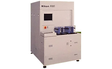
- AMI-2000 automatic macro inspection system
- OPTISTATION-3100 wafer inspection system
|
| 2002 |
- Nikon Precision Shanghai Co., Ltd. is established in China.
- Number of semiconductor lithography systems sold reaches 7,000.
- NSR-S206D (resolution ≦ 110 nm)
- NRM-3100 overlay measurement system
- AMI-3000 automatic macro inspection system
- N-SISⅢ illumination equipment for solid-state imaging device
|
| 2003 |
- NSR-S307E (resolution ≦ 80 nm)
- NSR-SF130 (resolution ≦ 280 nm)
- OPTISTATION-3200 wafer inspection system
|
| 2004 |
- NSR-S308F (resolution ≦ 65 nm)
- NSR-S208D (resolution ≦ 110 nm)
- Sales of POLANO polarized illumination technology for semiconductor lithography systems start.
|
| 2005 |
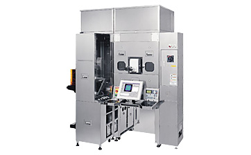
- NSR-S609B (resolution ≦ 55 nm), ArF immersion scanner for high-volume manufacturing with NA 1.07 (first scanner to break NA 1.0 threshold in the world)
- NSR-SF140 (resolution ≦ 280 nm)
- Number of semiconductor lithography systems sold reaches 8,000.
- N-SISⅤ illumination equipment for solid-state imaging device
|
| 2006 |
- NSR-S610C (resolution ≦ 45 nm)
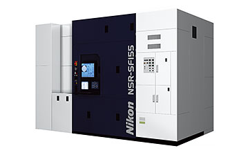
- NSR-SF155 (resolution ≦ 280 nm)
- OPTISTATION-3000 wafer inspection system
|
| 2007 |
- Tochigi Nikon Precision Co., Ltd. is established.
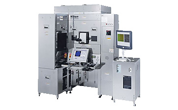
- NSR-S310F (resolution ≦ 65 nm)
- NSR-S210D (resolution ≦ 110 nm)
|
| 2008 |
- Sendai Nikon Precision Corporation is established.
- NSR-S620D (resolution ≦ 38 nm), ArF immersion scanner with the Streamlign platform
|
| 2009 |
- Mito Nikon Precision Corporation is merged with Tochigi Nikon Precision Co., Ltd.
- Sendai Nikon Precision Corporation is merged with Miyagi Nikon Precision Co., Ltd.
- NES1-h04 mini stepper
|
| 2011 |
- NSR-S320F (resolution ≦ 65 nm), dry ArF scanner with the Streamlign platform
- AMI-3500 automatic macro inspection system
|
| 2012 |
- NSR-S621D (resolution ≦ 38 nm)
- AMI-3000 MARKⅡ automatic macro inspection system
|
| 2013 |
- Nikon Precision Singapore Pte Ltd is merged with Nikon Singapore Pte. Ltd.
- NSR-S622D (resolution ≦ 38 nm)
|
| 2014 |
- Nikon Head Office is relocated to Shinagawa Intercity.
- NSR-S630D (resolution ≦ 38 nm)
- NSR-S322F (resolution ≦ 65 nm)
- NES1W-ih06/i06 mini stepper
- NES2W-ih06/i06 mini stepper
|
| 2015 |
- 450 mm ArF immersion scanner at the SUNY Polytechnic Institute transitions to wafer patterning.
- N-SIS8 illumination system for image sensor inspection
|
| 2016 |
- NSR-S631E (resolution ≦ 38 nm)
- NSR-S220D (resolution ≦ 110 nm)
|
| 2017 |
- AMI-5600 automatic macro inspection system
|
| 2018 |
- NSR-S635E (resolution ≦ 38 nm)
|
| 2019 |
- N-SIS9 illumination system for image sensor inspection
|
| 2021 |
- AMI-5700 automatic macro inspection system
|
| 2023 |
- Nikon Instruments (Shanghai) Co., Ltd. is merged with Nikon Precision Shanghai Co., Ltd., and corporate name is changed to Nikon Precision (Shanghai) Co., Ltd.
- Nikon Precision Malaysia Sdn. Bhd. is established in Malaysia.
- NSR-S625E (resolution ≦ 38 nm)
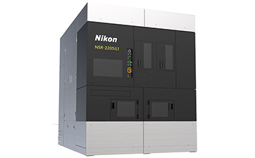
- NSR-2205iL1 (resolution ≦ 350 nm)
- NSR-S636E (resolution ≦ 38 nm)
|
| 2024 |
- Nikon Head Office is relocated to Nishioi, Shinagawa-ku, Tokyo.
|
| 2025 |
- Digital Lithography System DSP-100 (resolution 1.0 µm L/S)
- NSR-S333F (resolution ≦ 65 nm)
|