The Ultra Micro-NIKKOR:
The Industrial Lens That Laid the Foundation for Japan's Semiconductor Industry
No.9 | 1964 | In Pursuit of the "Ultrafine"
In 1964, a lens was born in pursuit of ultimate resolving power.
What began as lens manufacturing technology for a specialized industrial application eventually became the foundation for an era in which Japan was known as a "semiconductor powerhouse".
Why did a lens designed to observe a tiny world gain the power to transform an entire industry?
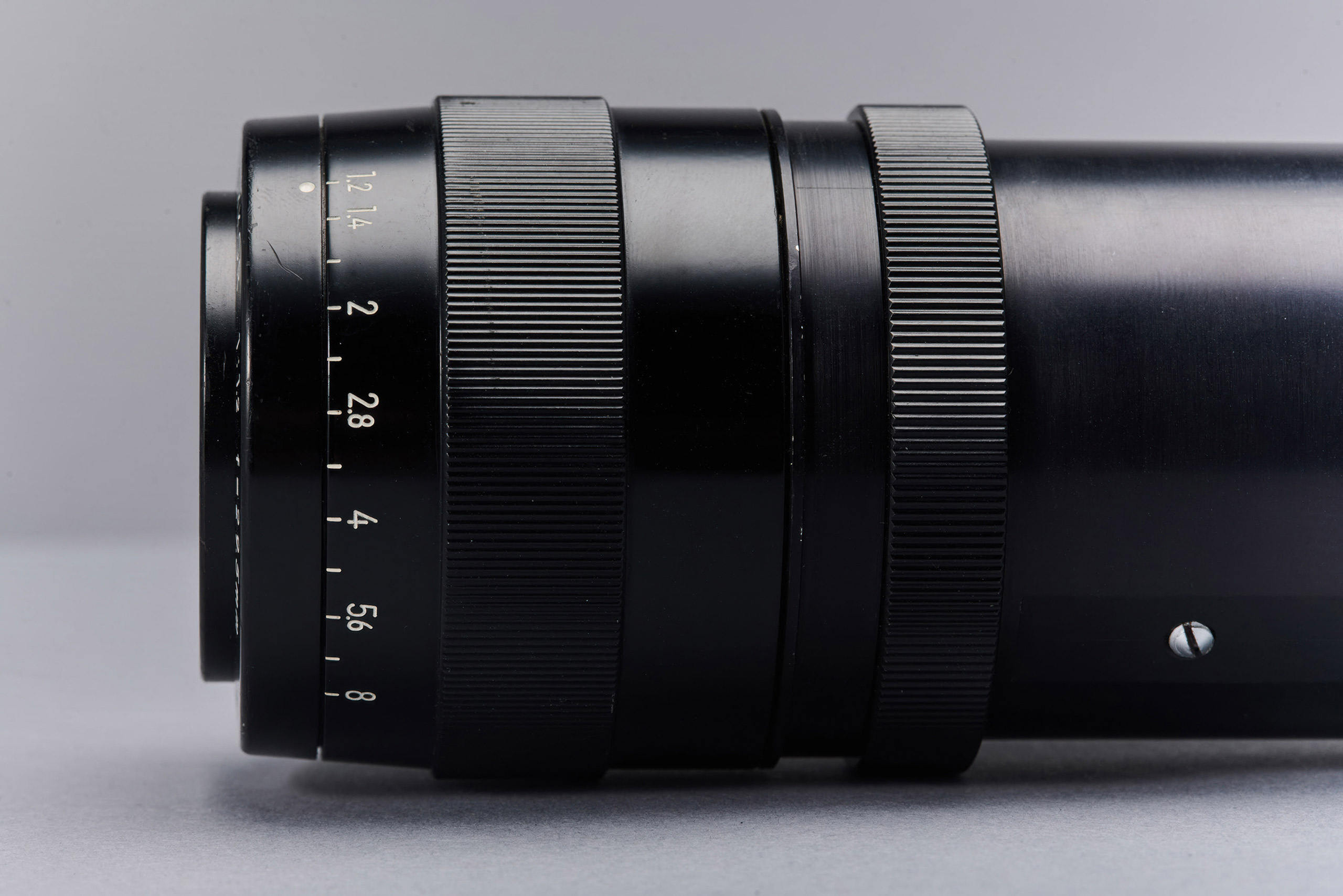
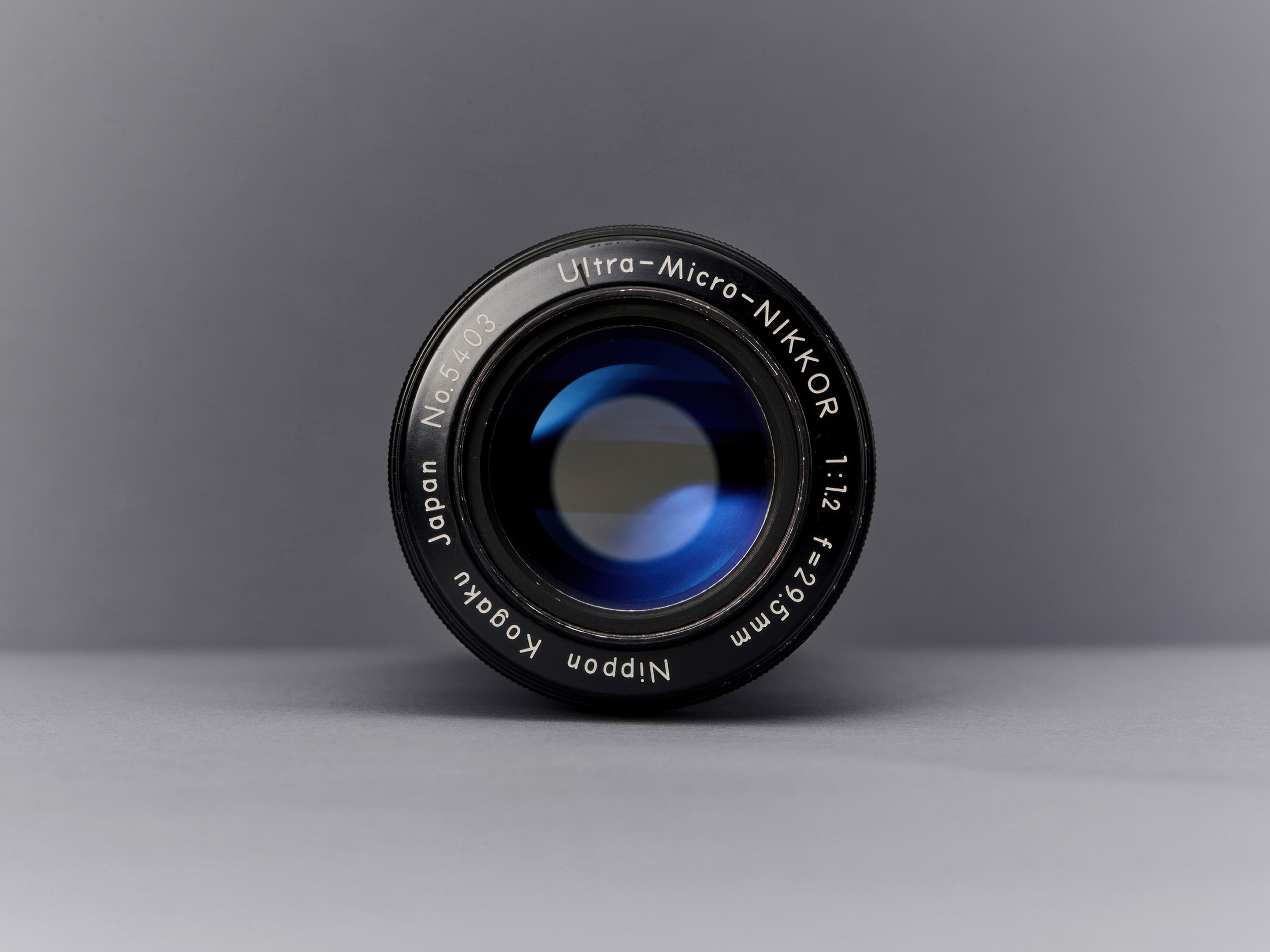
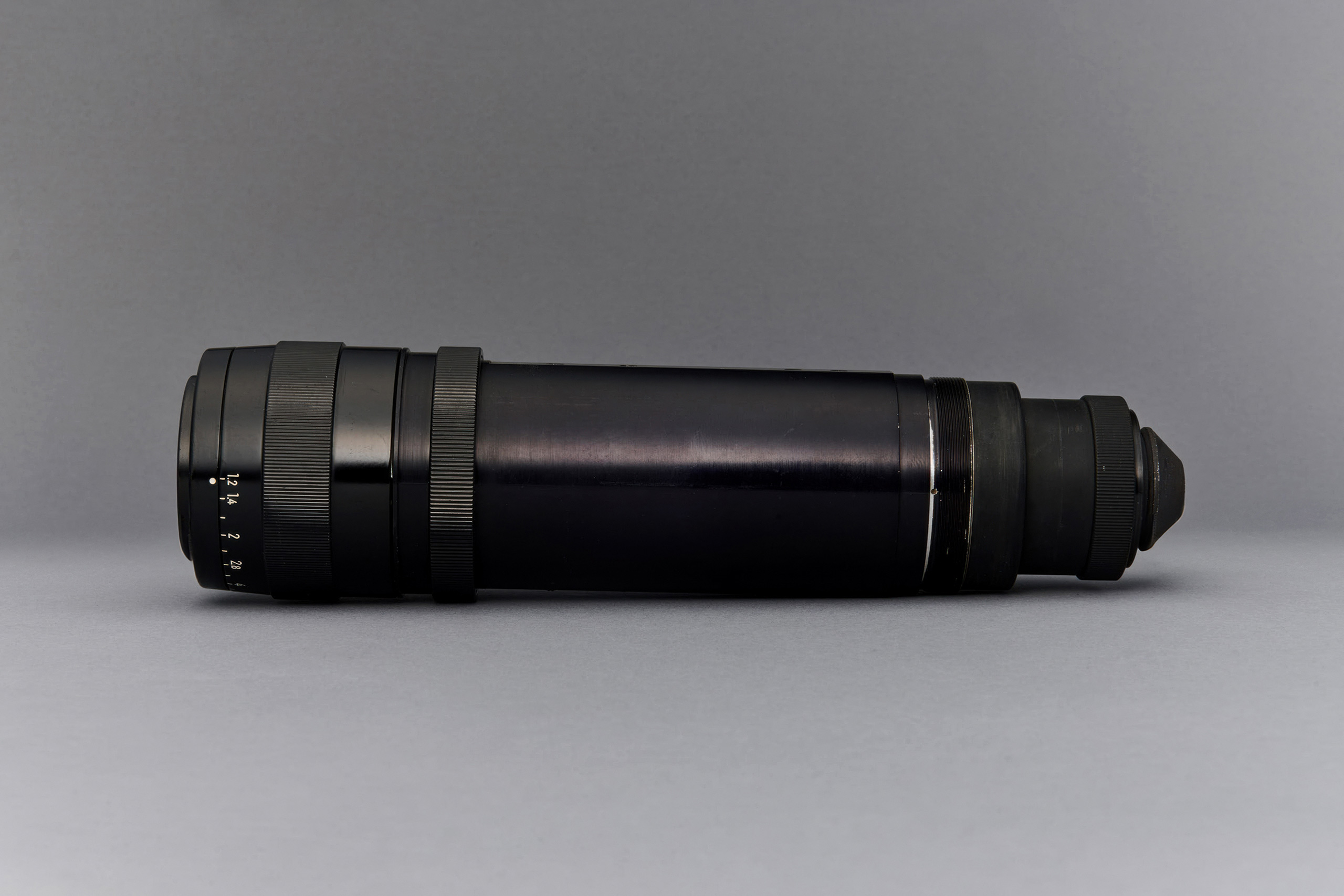
In November 1964, a single lens overturned the conventional wisdom of photography. The Ultra Micro-NIKKOR 29.5mm F1.2 achieved a resolution of 1,260 lines per millimeter — far beyond what had been thought possible at the time.
Until then, photographic lenses were believed to have a practical resolution limit of about 300 lines/mm, but this lens instantly delivered more than four times that performance.
Using this lens, an entire 350-page book was photographed and miniaturized onto an area the size of a then-10-yen postage stamp (22.5 x 18.5 mm), and then successfully enlarged back to its original size with the same lens, preserving the original resolution.
This feat was presented at the International Optical Congress in September 1964, causing a worldwide sensation among researchers and engineers.
A Challenge Born from Niche Demand
Yet, the development of this lens was never intended as a flashy technology demonstration.
It began with a few highly specific inquiries from printing companies and electronics manufacturers around 1960.
At that time, large printing companies — skilled in photographic plate-making — were increasingly producing the photomasks (the photographic originals for circuit patterns) that were required to manufacture semiconductors. However, the existing plate-making lenses could not effectively meet the precision demanded by the electronics industry. This sparked a call for lenses with far higher resolving power.
In March 1961, Nikon began development of a high-resolution lens for this very special application — photomask production — taking on a challenge in an entirely different realm from ordinary camera lenses.
To achieve higher resolution, it was essential to lower the f-number, which meant creating a lens with a large aperture ratio.
But at the time, correcting aberrations in such lenses was considered to be extremely difficult, or even impossible.
The key breakthrough originated from advice given by a researcher.
"If you use monochromatic light, the aberrations should be correctable," he suggested, completely shattering the development team members' previous assumptions.
By specializing the lens for the e-line (546 nm) of a mercury lamp — a monochromatic light source — they eliminated chromatic aberration, the biggest obstacle.
It was precisely because the lens was tailored to a limited, specific purpose that they could pursue its ultimate performance.
Technology that Captured the World's Attention
The first prototype, a 105mm F2.8 completed in August 1962, achieved a resolution of 400 lines/mm.
Then, to meet a demand for "over 1,000 lines/mm," the team developed the 29.5mm F1.2, which ultimately reached an unprecedented 1,260 lines/mm — the highest resolution in the world at that time.
When this lens — originally developed for the narrow application of photomask production only in Japan — was announced, it quickly drew widespread attention in the industry because of its exceptional capabilities.
However, the most astonishing response came from across the Pacific Ocean.
A semiconductor manufacturing equipment maker in the United States, which was the world leader in that field at the time, began sending Nikon requests for new lenses one after another.
A technology created to meet a niche domestic demand was now attracting the attention of the world's top players.

Technology Leads the Way to a Future Beyond Imagination
The expertise cultivated through the Ultra Micro-NIKKOR eventually became the foundation for Nikon's entry into the semiconductor manufacturing equipment business.
This lens paved the way for the development of the projection mask printer in 1969 and the commercialization of semiconductor lithography systems in 1980 — after a journey that began with the specialized need to produce photomasks.
However, how many people at the time could have predicted the huge industrial impact that these developments would eventually make worldwide?
Technology often evolves beyond the original intent of its creators.
A skill honed to the extreme for a single, limited purpose can unlock amazing new possibilities in totally unexpected fields.
The story of the Ultra Micro-NIKKOR perfectly illustrates this unforeseen power of technological development.
The ripples that emanated from the creation of a single lens eventually reached the computers and smart devices that surround us all today.
Beyond the blueprints envisioned by engineers lies a future that no one can fully predict.
Contents supervisor: WIRED JAPAN, Japanese text: Hideto Mizutani, Photography: Junpei Kato, Editing: Shinya Yashiro
Frontiers of Vision
- The Nikon Photomic FTN: A Camera for the Ultimate Shooting Environment — Space
- The Ultra Micro-NIKKOR: The Industrial Lens That Laid the Foundation for Japan’s Semiconductor Industry
- The D1 camera: Transforming professional workplaces into the digital era
- The COOLPIX 900: Paving the way for digital shooting
- The NIKONOS all-weather camera: capturing the world in any conditions
- The profile projector: the unsung equipment supporting the precision of manufacturing
- The COOLSCAN: A “personal × digital” realm created by digitalization
- The JOICO microscope: The challenge of peering deeply into the world
- The COOLPIX 300: Pursuing the technological possibilities of a multimedia recorder
- The MIKRON 6×: Compact binoculars born over 100 years ago