
Selected for NEDO's "Research and Development Project of the Enhanced Infrastructures for Post-5G Information and Communication Systems / Development of Manufacturing Technologies for Advanced Semiconductors (Subsidy)"
Nikon Begins Development of Digital Lithography System with 0.5 μm (L/S) Resolution
October 20, 2026
TOKYO - Nikon Corporation is pleased to announce that it has been selected for the "Research and Development Project of the Enhanced Infrastructures for Post-5G Information and Communication Systems / Development of Manufacturing Technologies for Advanced Semiconductors (Subsidy)" conducted by the New Energy and Industrial Technology Development Organization (NEDO) for its newly launched development of a digital lithography system capable of achieving 0.5 µm*1 (L/S)*2 resolution.
This project aims to develop the core technologies that will underpin information and communication systems supporting the post-5G era. Through these efforts, it seeks to strengthen the development and manufacturing foundations of post-5G information and communication systems while simultaneously achieving both a digital society and decarbonization. NEDO has selected Nikon's proposal to develop a high-resolution digital lithography system for advanced packaging, submitted under the topic of "large-area, high-precision exposure system development" for advanced semiconductor manufacturing equipment.
Development of high-performance semiconductor devices is accelerating in order to address challenges such as growing data volumes driven by the widespread adoption of post-5G — a next-generation communications technology — and AI, as well as the need to reduce the associated power consumption. Technological innovation is currently advancing in the back-end semiconductor device manufacturing process (advanced packaging). In panel-level packaging, exposure technology capable of forming high-resolution, high-density redistribution layers (RDL) on large substrates is becoming increasingly important.
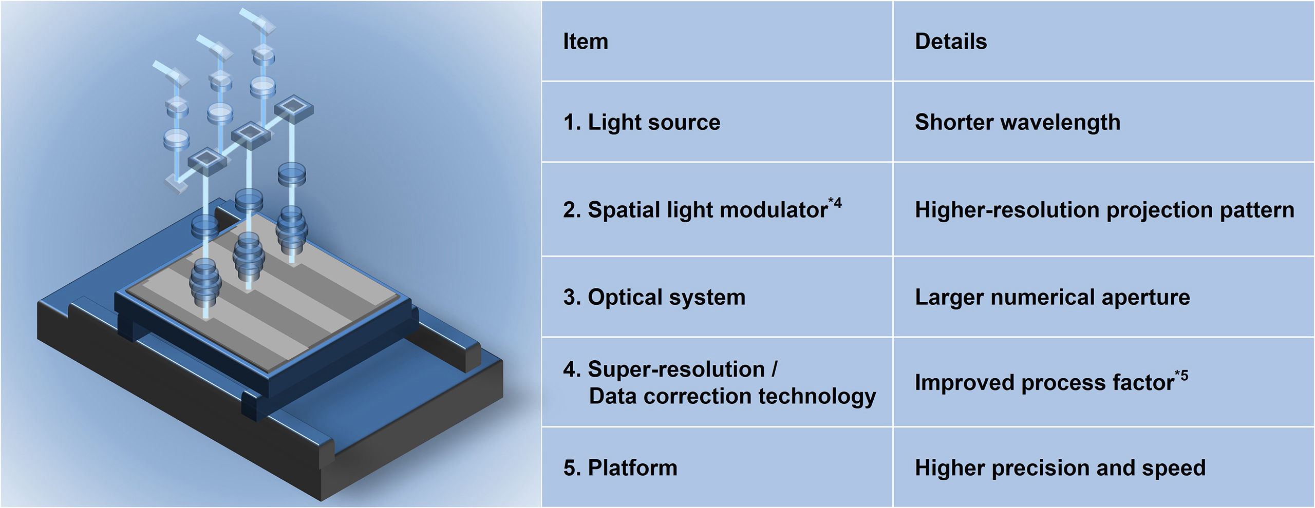
In its current Medium-Term Management Plan, Nikon has identified digital lithography systems as one of its focus areas. To date, the company has developed digital lithography systems with resolutions of 1.0 µm and 1.5 µm (L/S) and overlay accuracy of ±0.3 µm or less. Through this selection, Nikon will further improve resolution, precision, and productivity by developing a digital lithography system that achieves resolution of 0.5 µm (L/S), overlay accuracy of ±0.15 µm or less, and a 50% reduction in energy consumption compared to conventional systems. *3
- 1 µm (micrometer) is one-millionth of a meter (one-thousandth of a millimeter).
- Abbreviation of line-and-space. Refers to the width of circuit lines and the spacing between adjacent patterns.
- Based on 510×515 mm substrates
- Optical device that displays a circuit pattern instead of a conventional photomask in a maskless exposure system.
- A proportionality constant that determines circuit resolution in the exposure process. A lower value is required to achieve circuit miniaturization.
The information is current as of the date of publication. It is subject to change without notice.