
Product name
Nikon Begins Accepting Orders for the FX-6ASLH, the World's First Submicron-Resolution FPD Lithography System
Achieving 0.85 µm (L/S) resolution
October 26, 2026
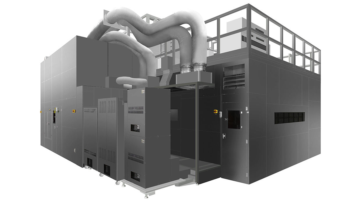
TOKYO -Nikon Corporation (Nikon) has begun accepting orders for the FX-6ASLH, an FPD lithography system that achieves 0.85 µm*1*2 (L/S*3) resolution, becoming the world's first FPD lithography system to deliver submicron resolution.*4 The FX-6ASLH is designed for the G6 plate size*5 and is optimized for the production of high-definition OLED and LCD panels used in advanced smart devices.
*1: 1 µm (micrometer) represents one-millionth of a meter (one-thousandth of a millimeter).
*2: Resolution of 0.85 µm is achieved when using a phase-shift mask and chemically amplified resist.
*3: Abbreviation for "Line and Space." Refers to the width of circuit lines and the spacing between adjacent patterns.
*4: Based on Nikon research of publicly announced FPD lithography systems as of October 26, 2026.
*5: 1,500 mm × 1,850 mm glass substrates for small- and medium-sized panels.
Product name and release date
|
|
FPD lithography system FX-6ASLH |
|---|---|
|
Sales launch |
December 2027 |
Development background
As displays for advanced smart devices continue to evolve toward higher definition and greater functionality, FPD lithography systems supporting G6 plates for small- and medium-sized panels are increasingly required to achieve resolution below 1.0 µm (L/S). To address this demand, Nikon has newly developed the world's first FPD lithography system to achieve high resolution of 0.85 µm.
Key features
1. Achieves 0.85 µm (L/S) resolution
By employing a newly developed illumination optical system incorporating a UV-LED light source, the FX-6ASLH achieves resolutions of 0.85 µm (L/S) and 1.0 µm (C/H)*6 on G6 plates. This represents the first submicron resolution achieved by an FPD lithography system. Even on large plates more prone to distortion, the system can perform exposure across the entire substrate with uniform linewidths while correcting focus in real time.
*6: Abbreviation for "Contact Hole." Refers to the diameter of holes used to electrically connect upper and lower layers.
2. Achieves overlay accuracy of ±0.18 µm or better
By precisely controlling each lens in Nikon's multi-lens system*7 according to substrate conditions and by carefully managing the operating environment within the system, the FX-6ASLH achieves overlay accuracy of ±0.18 µm or better, representing the highest level*8 among FPD lithography systems supporting G6 plates. This contributes to achieving high-yield mass-production processes.
*7: Nikon's proprietary technology that precisely controls multiple projection lenses to perform exposure as though using one large lens, enabling wide-area patterning in a single exposure.
*8: Based on Nikon research of publicly announced FPD lithography systems as of October 26, 2026.
3. Provides high resolution and high productivity by using a UV-LED light source.
The adoption of a high-intensity UV-LED light source enables both submicron resolution and high productivity, delivering outstanding overall performance.
Performance overview
 Swipe horizontally to view full table.
|
Resolution |
0.85 µm L/S*3, 1.0 µm C/H |
|---|---|
|
Light source |
UV-LED i-line equivalent |
|
Projection magnification |
1 : 1 |
|
Overlay accuracy |
≤± 0.18 µm |
|
Plate size |
1,500 mm × 1,850 mm |
|
Takt time |
39 s/plate |
The information is current as of the date of publication. It is subject to change without notice.