Advancing Semiconductor
Manufacturing Through Digital Lithography


Our everyday lives are constantly being enriched by new digital technology. From generative AI to video streaming to cloud services, these innovations are driving an incredible surge in data and placing unprecedented demands on both the data centers and the semiconductors that power them.
Drawing on decades of expertise in both semiconductor and FPD (flat panel display) lithography systems, Nikon has developed the Digital Lithography System DSP-100, introducing a new approach to semiconductor manufacturing.
A New Approach to Advancing Semiconductor Miniaturization
Semiconductors are essential to many different industries; from the electronics we use every day to key infrastructure. As digitalization continues to accelerate, it is becoming a key driver behind the growing demand for semiconductors.
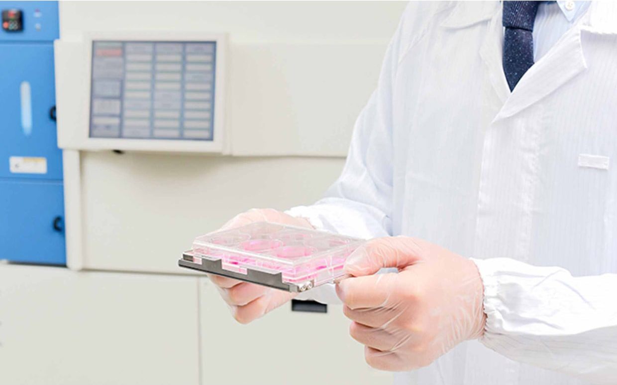
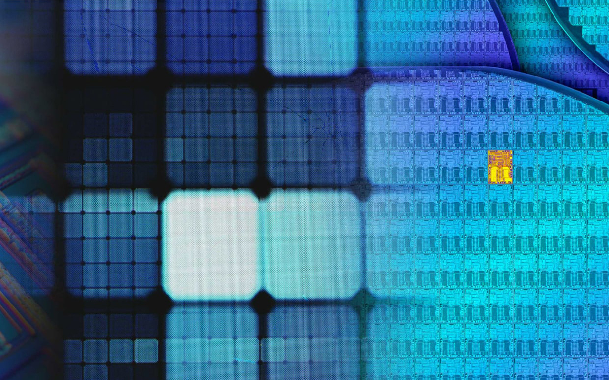
Semiconductor manufacturing consists of two major stages: front-end and back-end processing. The front-end process involves repeatedly forming thin films and performing photolithography using lithography equipment to etch intricate circuit patterns onto silicon wafers. During the back-end process, these wafers are diced into individual chips and packaged.
Until now, circuit miniaturization during front-end processing has driven improvements in semiconductor performance. However, as the technical challenges of further miniaturization continue to intensify, new approaches are required. One promising approach lies in advanced packaging, a back-end technology that enhances semiconductor performance through methods other than miniaturization. By combining multiple chips at high density, advanced packaging can effectively enhance performance while also saving energy and costs.
Nikon believes that the expertise it had built over the years could create new value, not only in front-end miniaturization, where it had long been a key contributor, but also in advanced packaging for back-end processing.
Nikon's First Venture into Back-End Lithography

In conventional lithography systems for advanced packaging, "step-and-repeat lithography," a mask-based projection process that transfers patterns from a photomask onto the substrate has long been the mainstream approach. However, as package sizes increase, more masks are required, reducing the overall productivity. Because the pattern size is physically limited by the dimensions of each mask, it is necessary to repeatedly switch masks and expose the substrate in multiple steps.
This is where "maskless lithography" proves highly effective. Rather than using photomasks, it employs a spatial light modulator* (SLM) to directly project circuit patterns, such as CAD data, directly onto substrates. By completely eliminating the need for masks, this approach not only significantly reduces the costs and lead time of semiconductor development and production, but also enables high productivity for large advanced packaging substrates, no longer constrained by photomask dimensions.
However, adopting a maskless lithography method alone is not sufficient to revolutionize advanced packaging. Successfully achieving that goal requires a highly sophisticated technological foundation within the lithography system itself.
For over 45 years, Nikon has developed and manufactured lithography systems, delivering more than 10,000 units across semiconductor (front-end) and FPD applications. The technological foundation built over those decades now drives new value in advanced packaging. The result is Nikon's first back-end lithography system: the Digital Lithography System DSP-100.
- *A device that electronically controls light amplitude, phase, and polarization.

A Fusion of Technologies Creating a Unique Advantage
The DSP-100 is supported by four main technologies: the previously mentioned "maskless lithography," "high resolution," "multi-lens technology," and "high-speed stage technology."
Foremost is high-resolution technology. The resolution of the lithography system is critical for forming fine circuit patterns. Drawing on the expertise refined through its semiconductor lithography systems, Nikon has the optical design technologies to achieve nanometer-level resolution, enabling the DSP-100 to easily reach a resolution of 1.0 µm (L/S).
Alongside this, another major strength of the DSP-100 is Nikon's multi-lens technology, long utilized in its FPD lithography systems. When adopting a maskless lithography method for the DSP-100, Nikon recognized that conventional approaches still lacked sufficient productivity. To overcome this, multi-lens technology was applied. This technology precisely aligns and controls multiple lenses to expose large areas with high accuracy, playing a major role in achieving the high productivity of the DSP-100.
Furthermore, high-speed stage technology has also made a significant contribution to productivity. In Nikon's FPD lithography systems, it enables a high processing capacity of 86 panels per hour for large substrates measuring 1,500 x 1,850 mm. This technology has been applied to the DSP-100.
Although the DSP-100 was gradually taking shape thanks to this technological expertise, realizing both high resolution and high productivity in optimal balance still remained as a major challenge. The biggest difficulty lay in processing the immense volume of data required to drive the SLM.
In digital lithography systems, the design data that defines the desired lithography pattern needs to be converted into drive data for actual lithography. As finer patterns require higher SLM resolution, the volume of drive data increases dramatically. Consequently, the time needed to convert design data into drive data also expands, inevitably reducing productivity. Nikon ultimately overcame this obstacle by developing a proprietary technology that allows high-speed data transfer to the SLM without sacrificing resolution. This breakthrough was key to surmounting the barrier.
Through this synergy of Nikon's advanced technologies, the DSP-100 back-end lithography system was successfully developed, providing an exceptional balance of resolution and productivity.


Opening a New Chapter in Semiconductor Manufacturing
Since its announcement, the DSP-100 has attracted strong interest from across a range of industries, including some that are outside of Nikon's previous business areas. This reflects the growing demand for higher-performance semiconductors in everyday products and services. To meet these needs, Nikon is currently conducting system evaluations with various customers in back-end processing, while development toward the next generation of digital lithography systems is also advancing.
With its expertise in both semiconductor and FPD lithography, Nikon is uniquely positioned to add new value to the back-end domain. The DSP-100 is set to play a key role in advancing semiconductor manufacturing, supporting the continued evolution of the devices and services that society relies on.

Next Generation Business Development Division, Precision Equipment Business
Takeshi Yaegaki
It's an exciting challenge to enter the back-end field, and I can feel a lot of enthusiasm around me as an engineer. We're pleased to see that our customers are expecting the system to play a key role in advanced packaging and are optimistic that Nikon can make it happen. We are fully committed to meeting their expectations and helping to create a new era in semiconductor manufacturing.
Optical Engineering Division
Daiyu Fujii
We believe that the demand for features such as high resolution, overlay accuracy, and productivity will increase even more in the future. We fully understand that these factors often involve trade-offs, so our mission is to accurately assess customer needs and market trends. That way, we can continue creating systems that will deliver greater value for them.

Product Strategy Division, Precision Equipment Business
Shunya Nishizawa
In semiconductor manufacturing, particularly in the back-end processing market for advanced packaging, standards for substrate size and package structure have yet to be established. As a result, the specifications required for the DSP-100 differ greatly from one customer to another.
This is why we make a point of communicating closely not only with our customers, but also with materials and equipment manufacturers involved in related processes. By seeing the whole picture, we can better understand the kind of value each customer truly needs and how to maximize it. Moving forward, we hope to deliver lithography systems that genuinely support the entire semiconductor manufacturing industry by effectively connecting front-end and back-end technologies.
- *Divisions and responsibilities are as of the time of the interviews.
For more information on the system
Originally published: March 31, 2026.


