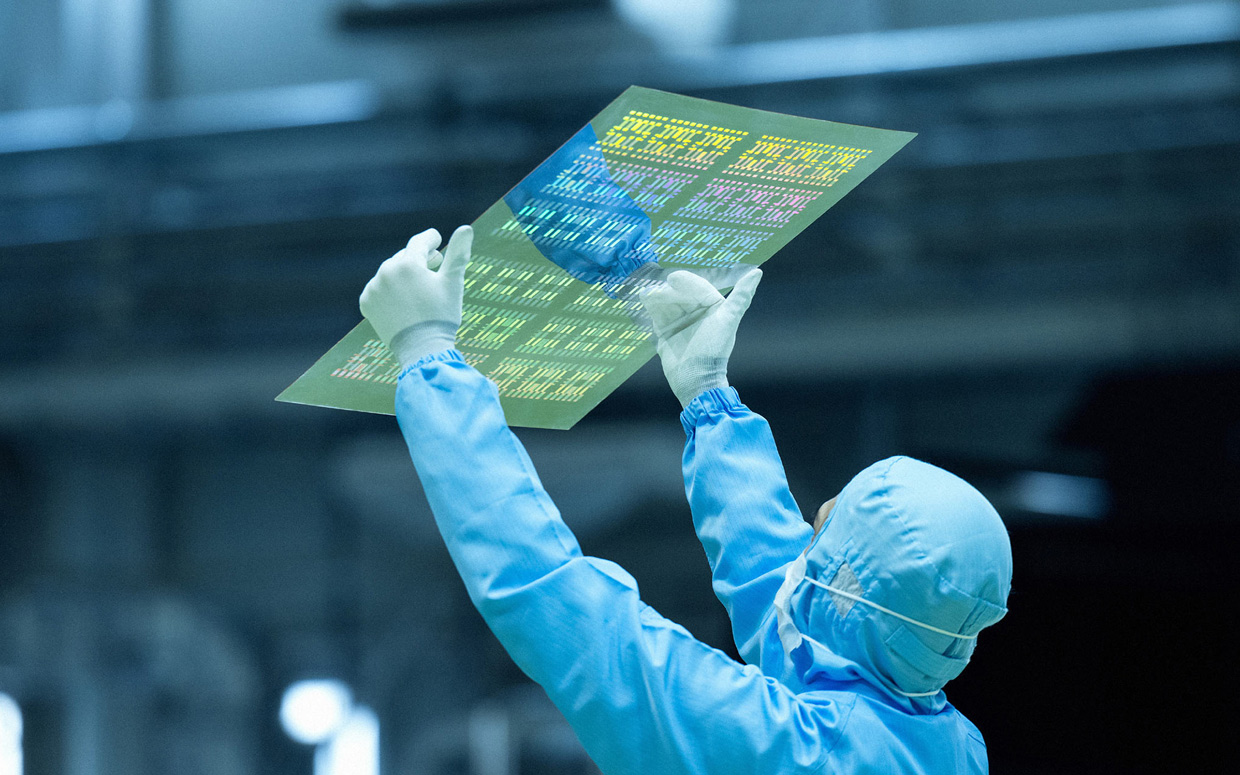
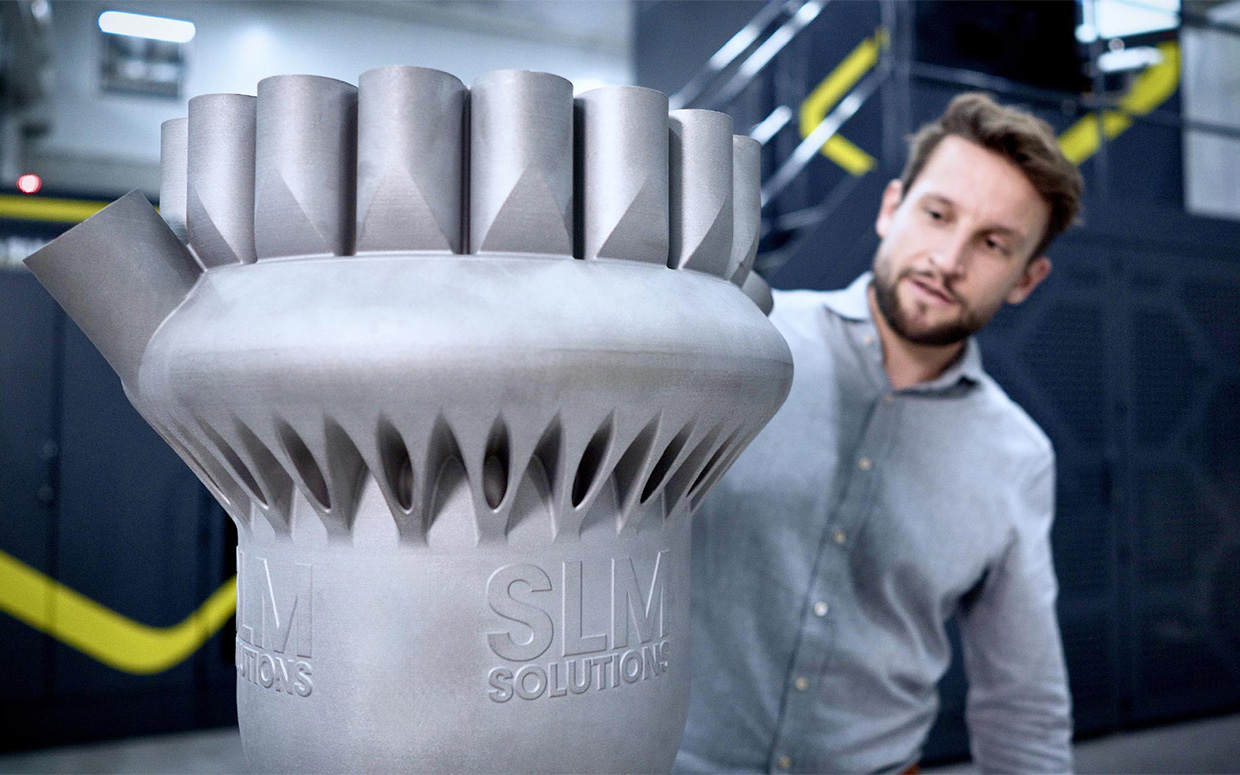
The further development of society through semiconductor manufacturing

Semiconductor lithography systems
that pave the way to a super-smart society
From small devices such as smartphones to large products such as automobiles,
everything in our society is becoming smarter.
Semiconductors are an essential part of such a smart society.
Nikon's semiconductor lithography systems
greatly contribute to the manufacture of these semiconductors.
Diverse semiconductors for a diversity of products

Since around 2020, many industries have been affected by a global shortage of semiconductors. There are many reasons for this, but the main root cause can be traced back to the great demand for them.
Today, semiconductors can be found in all kinds of items, from small devices such as smartphones, to large products like automobiles. A variety of semiconductors are used in them, and it is impossible to complete them with just one kind of semiconductor.
Let's take automobiles as an example. The advancement of 'automation', in which vehicles judge their surroundings by themselves to support driving, and 'electrification', in which cars run on motors instead of engines to reduce CO2 emissions, is progressing every day. In this evolution of the automotive world, semiconductors play an important role.
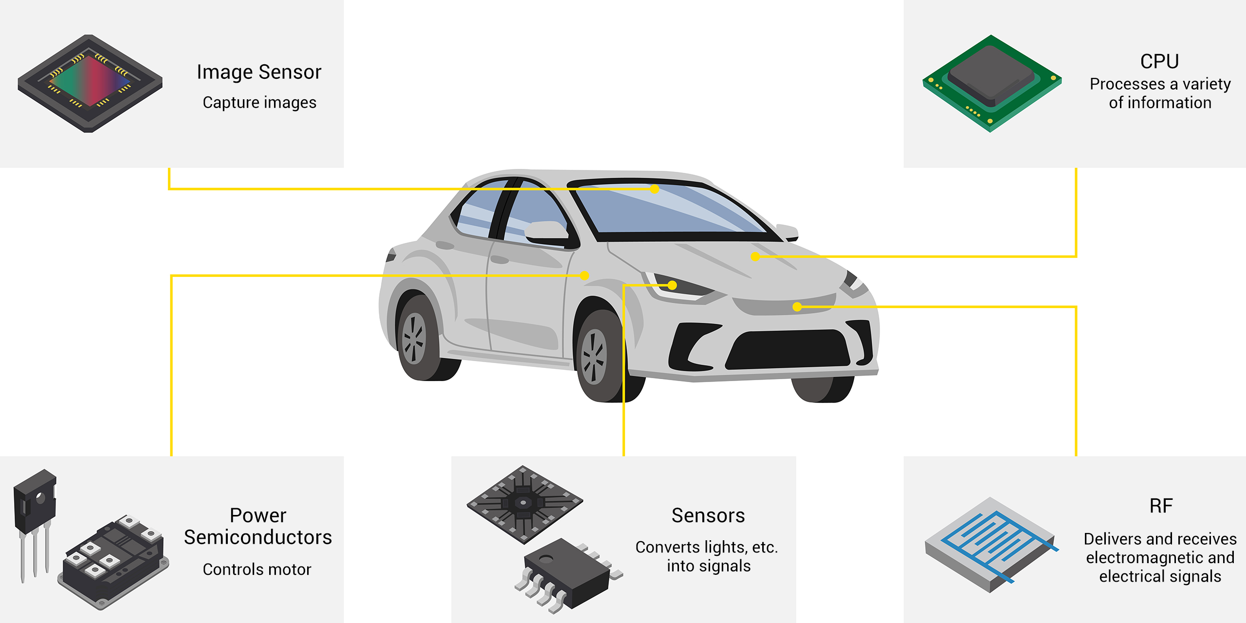
For instance, car sensors are equivalent to the eyes of humans, allowing the car to locate pedestrians and other cars. The CPU determines danger, as does the human brain. Power semiconductors* act in the same way as our muscles, controlling the tires, steering, and brakes, via the information received.
In addition to this, automobiles are equipped with countless semiconductors, such as those for communication, audio, and many others, to the extent that automobiles are sometimes regarded as 'semiconductors on wheels'.
As represented by automobiles, machines are becoming ever more intelligent. They are supporting people by seeing, hearing, thinking, and moving independently. Semiconductors have become an indispensable part of our society and Nikon plays an important role in their manufacturing process.
- *A semiconductor device that can convert or control power.
Semiconductor lithography systems are a key component in the manufacture of semiconductors
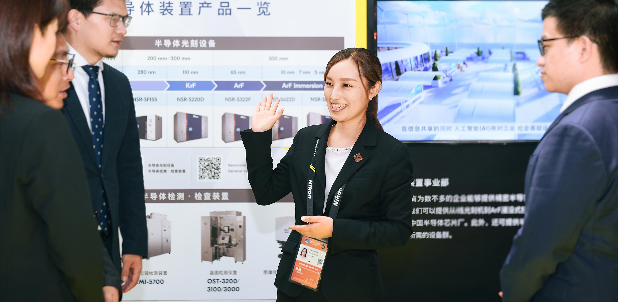
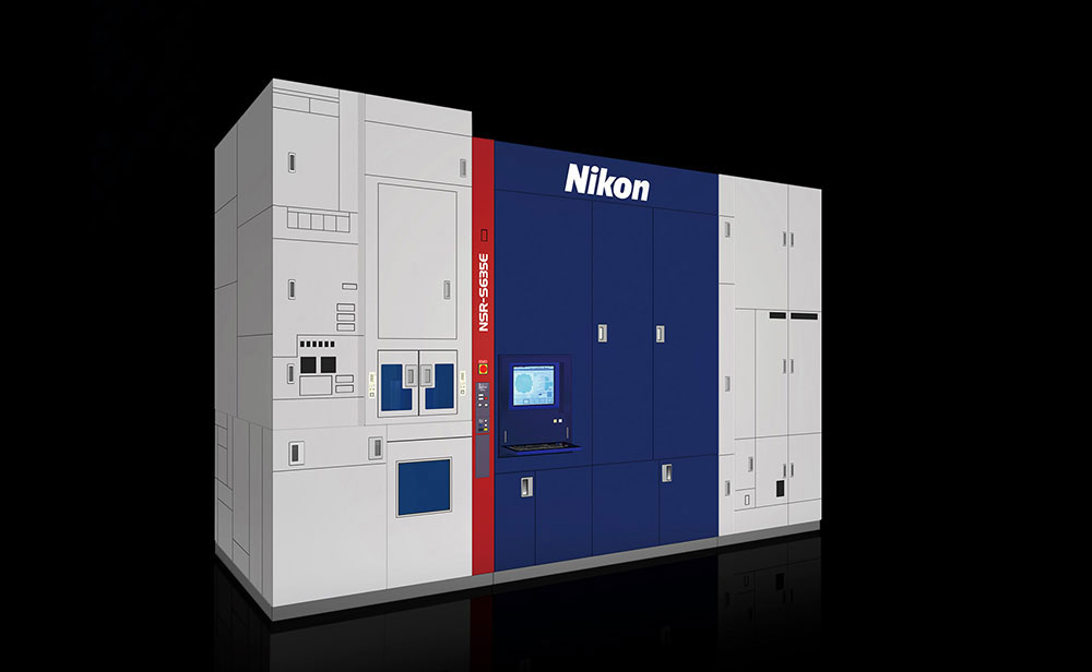
Nikon manufactures semiconductor lithography systems, also known as the 'most precise machine in history'. These systems etch circuits onto circuit boards and play one of the most important roles in the semiconductor manufacturing process.
Given the great variety of semiconductors playing different roles, the systems used to manufacture them are also diverse.
Semiconductors are broadly divided by the widths of the circuits drawn on the circuit boards, into the 'ultra-fine type' and 'non-ultra-fine type', and the devices have difference areas of specialties for each.
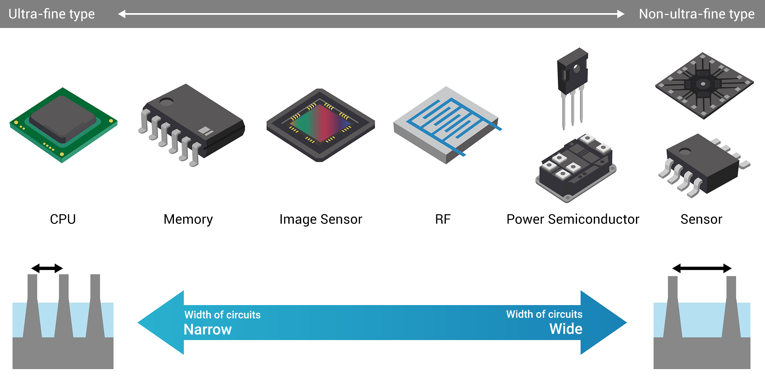
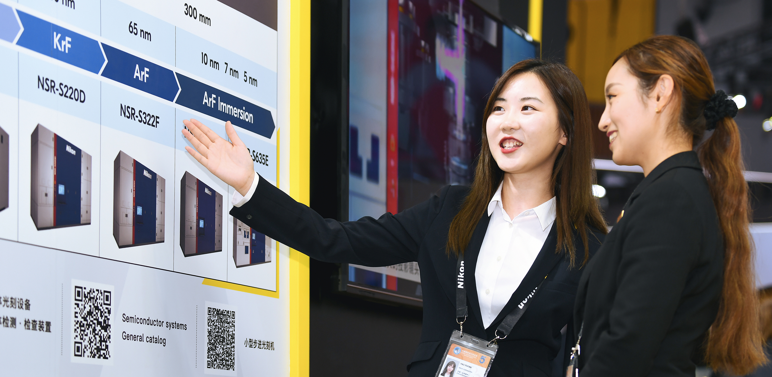
We are told by Ms. Feifan Yao, a representative from the sales team that "Nikon provides a wide lineup of lithography systems for producing diverse types of semiconductors, from narrow circuit widths of 'ultra-fine types' to wide circuit widths of 'non-ultra-fine types', to meet the specific manufactured semiconductor requirements of our customers. We also provide equipment for the measurement and inspection required during the manufacturing process, as well as offering a variety of devices for the manufacture of different semiconductors."
"In terms of Nikon's semiconductor lithography systems, the ArF type mainly produces the 'ultra-fine types' of semiconductors. It utilizes the ArF laser, a short wavelength light, making it possible to etch fine circuits on circuit boards.Even just within 'ultra-fine types' of semiconductors, there are different levels of fineness, and the ArF type system is responsible for the etching process of the finest circuits for these."
This system manufactures logic semiconductors, such as CPUs, and memories for data storage, mainly those equivalent to the functions of a human brain.
Lithography Systems

Metrology/Inspection Systems

"On the other hand, 'image sensors', which correspond to the human eye, and 'power semiconductors', which correspond to muscles, are classified as 'non-ultra-fine types'. They are mainly manufactured with KrF lasers and i-lines, which have long light wavelengths."
With its foundation of development from more than 100 years of refining opto-electrics technologies, Nikon has been developing systems that can effectively correspond to the manufacture of a diverse range of semiconductors.
Ms. Chiemi Hoshino, a representative from the marketing department, explains this technology as follows.
"Nikon has continued to use opto-electronics technology to pursue observation of microscopic items that are invisible to the human eye, and capture images. You could say that our semiconductor lithography systems are one of the achievements of these efforts. But the development of both semiconductors and semiconductor lithography systems is still evolving. We will continue to take part in this evolution by freely controlling light."
The continual evolution of semiconductors and semiconductor lithography systems
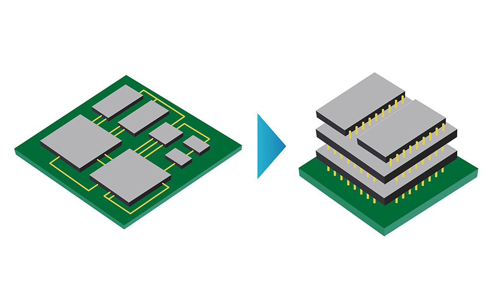
The evolution of semiconductors, as well as their different possibilities with the two categories of 'ultra-fine types' and 'non-ultra-fine types' is still being explored.
Firstly, making semiconductors 'three-dimensional' is the focus of attention for the development of 'ultra-fine types' such as CPUs and memories. There are different methods employed to achieve this, including stacking the chips and changing the circuit design from a two-dimensional structure to three dimensions. In order to improve the performance while reducing costs, the technology put into the system, along with the fineness of the circuits themselves is constantly evolving. However, Mr. Tasuku Kato, another representative from the marketing department, explains that even though there are still challenges for 3D semiconductors that did not exist in the conventional manufacturing process, they can see the light at the end of the tunnel.
"The manufacturing process is very vulnerable to the effects of pressure and heat, and slight distortions can occur. They may be so small as to be invisible to the human eye, but can cause fatal problems in the world of semiconductors. However, if such distortion can be captured precisely, it can be corrected during the lithography process. At Nikon, there are technologies such as the Litho Booster and inline Alignment Station (iAS), which measure the distortion before the lithography process, and feed this data forward to the lithography system. With the use of these technologies, I believe that even higher precision and productivity can be realized."
In the trend of development for 'non-ultra-fine types' such as power semiconductors, in addition to making them three-dimensional, the capability of accommodating to new materials is also focused on. The use of silicon carbide (SiC) has been increasing for power-saving and handling high power. Silicon, that has been widely used in the past, was unable to achieve this. As semiconductors generate heat when in operation, using silicon carbide can control the heat more effectively than silicon, and thus provide longer durability.
If these technologies are adopted in electric vehicles, it will be possible to increase the charging speed, lose less of the stored electricity to convert into power, and thus further extend the driving distance.
Mr. Kato goes on to say, "Silicon carbide possesses different physical properties as a material for semiconductors from silicon and requires lithography systems to take care of the distortions created during the manufacturing process. It may sound simple, but with demands in nanometer-units, even seemingly simple matters can become difficult. Nikon is also utilizing the precision technology it has developed over the years to support these new materials."
Both Mr. Kato and Ms. Hoshino state that it is Nikon's stance to continue to equally pursue the advancement of both 'ultra-fine types' and 'non-ultra-fine types'.
Semiconductors and society are both truly interrelated. People make semiconductors to enrich society and semiconductors exceed the capabilities of people, thus improving our quality of life. For the further development of semiconductors and society, Nikon continues to take on challenges to create a better future as a semiconductor lithography manufacturer.
For a future yet to be seen
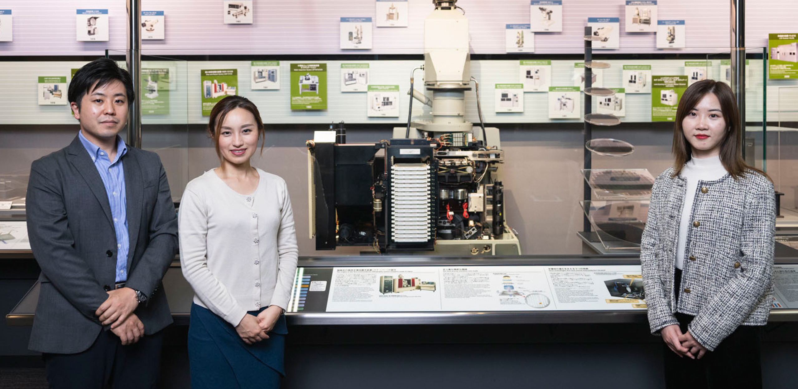

Tasuku Kato
Semiconductor Lithography Business Unit
"We want to incorporate as much customer feedback as possible into our products. Compared to the past, the use of semiconductors has greatly increased in the areas they are applied to. They are key devices to provide us with a more convenient and enriched life. Nothing would make us happier than to be able to contribute to our customers through our semiconductor lithography business.
And personally, as we have a large lineup of semiconductor lithography systems at Nikon, I am also able to be involved in a wide range of areas. These experiences are very rewarding, and I hope that we as a semiconductor lithography system manufacturer can continue to contribute to creating a brighter future."

Chiemi Hoshino
Semiconductor Lithography Business Unit
"Semiconductors hold even more possibilities than those we have realized already. Not only do I hope that more people will gain an understanding of this, but also that equipment manufacturers like Nikon will play an increasingly active role in the process of manufacturing semiconductors.
And we will also launch a new semiconductor lithography system in the not-too-distant future. It is not easy to pursue the development of both 'ultra-fine types' and 'non-ultra-fine types', but I believe that through our continuous efforts, there will be great new value that only Nikon can create."

Feifan Yao
Semiconductor Lithography Business Unit
"Based on Nikon's Medium-Term Management Plan, we have launched the 'partnering activities' project, in which teams are formed by region and customers managed, to understand deeply exactly what our customers are looking for and to closely support them. As opportunities for the use of semiconductors expand, Nikon's business is also expanding further worldwide. Our close support for customers does not change whether it is in Japan, China, or anywhere else. As a semiconductor lithography manufacturer, we will continue to respond to each customer's requests thoroughly and flexibly while keeping an eye on social trends."
- *Divisions and responsibilities are as of the time of the interviews.
Click here for the product lineup of semiconductor lithography systems and further information.
Originally published: Feb 6, 2023.

