Precision Equipment Business

Building a super-smart society
IC chips and high-resolution flat panel displays hold the key to further improvements in IoT and AI.
Through the development and production of manufacturing systems that expose circuit patterns of such components, Nikon is supporting the creation of a super-smart society.
Flat panel display (FPD) manufacturing process and FPD lithography systems

FPD lithography systems
FPD lithography systems project circuit patterns onto the surface of glass plates for controlling each pixel. Nikon provides diverse types of systems, from those employing the unique multi-lens system for handling large panels, to those for producing the small- and medium-sized panels such as those employed by smart devices. Nikon has achieved a high market share of FPD lithography systems by continuous technological development.
Semiconductor manufacturing process and semiconductor lithography systems

Semiconductor lithography systems
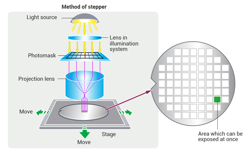
Semiconductor lithography systems reduce the size of circuit patterns and project them onto silicon wafers.
The systems, crucial to IC chip production, require an extreme precision down to 1 nm (one-billionth of a meter), and are regarded as the most precise machines ever developed.
Major products
FX-103SH FPD Scanner
The 10.5th generation FPD lithography system that has fully enhanced illumination and multi-lens systems that use Nikon's proprietary resolution enhancement techniques. It is optimized for manufacturing high-definition large-sized panels and mass-production of 4K and 8K TVs, as well as LCD panels for high-definition tablets and organic EL panels.
FX-6AS FPD Scanner
The FX-6AS is an optimal FPD lithography system for manufacturing high definition organic light emitting diode (OLED) panels and LCD panels for the latest and high-definition mobile devices, such as smartphones.
With the newly developed projection lens, the FX-6AS enables the highest level of resolution, high alignment accuracy, and high throughput. The FX-6AS employs an i-line light source that has been used in the existing models.
This enables the high-volume production of high definition panels without changing the existing manufacturing processes.
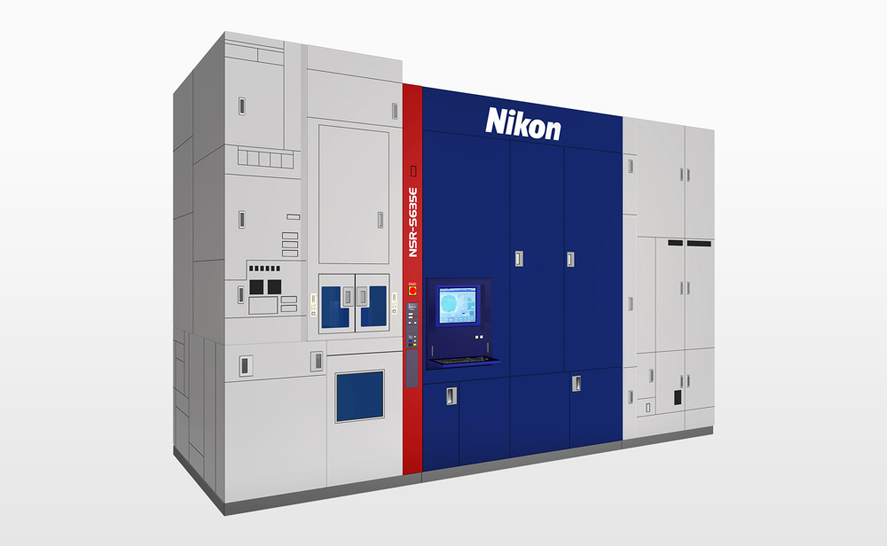
NSR-S635E ArF Immersion Scanner
The NSR-S635E adopts the Streamlign platform developed for high-volume 5 nm node application manufacturing. Integrating an inline Alignment Station, the NSR-S635E delivers remarkably high accuracy and productivity, providing overlay accuracy under 2.1 nm MMO and throughput of more than 275 WPH (96 shots) simultaneously. It greatly contributes to the stability of cutting-edge mass device production lines.
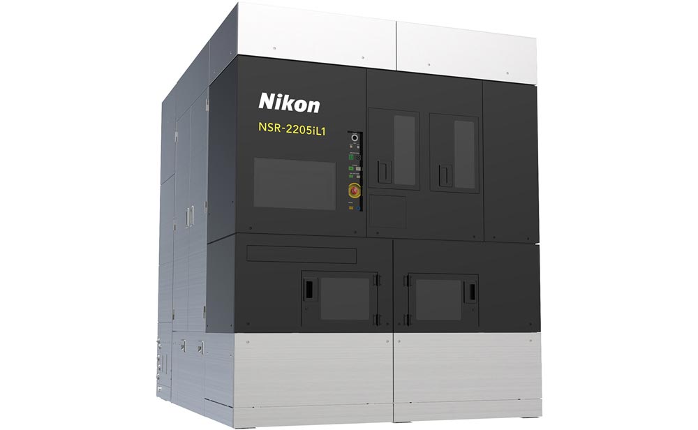
NSR-2205iL1 5x Reduction i-Line Stepper
The NSR-2205iL1 will be used to manufacture a variety of devices such as power and communications semiconductors and MEMS, and is fully compatible with existing Nikon i-line exposure systems.
It provides excellent affordability and will enable optimized production of various semiconductor devices regardless of the wafer material.
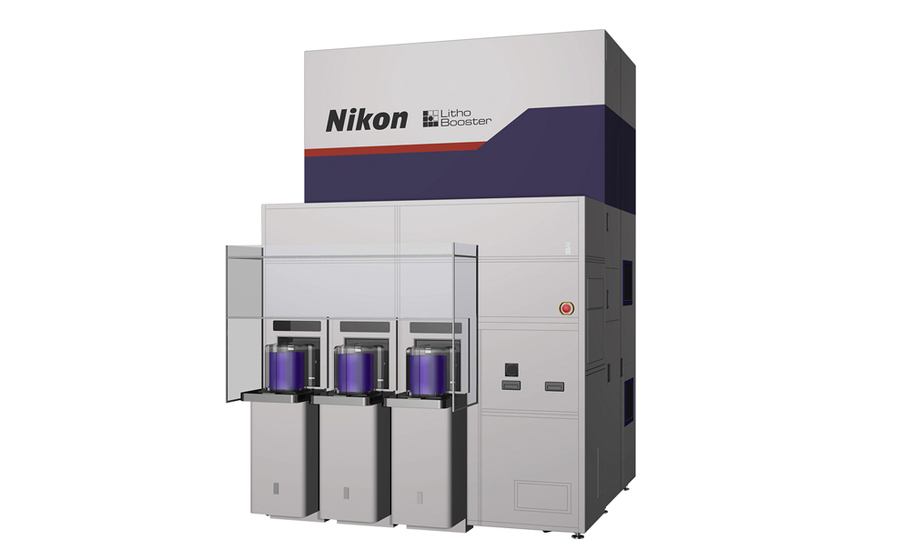
Litho Booster Alignment Station
The Litho Booster is an advanced Alignment Station that leverages proprietary Nikon technologies developed for semiconductor lithography systems. Absolute grid distortion values are measured quickly with ultra-high precision for all wafers prior to exposure. Correction values are then fed forward to the lithography system to greatly improve overlay accuracy without reducing throughput, contributing to enhanced yield and optimized equipment investment.