Nikon Announces 450 mm ArF Immersion Scanner at SUNY Polytechnic Institute is Transitioning to Wafer Patterning
July 9, 2015
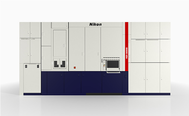
Nikon Corporation (Kazuo Ushida, President) announced the world's first ever 450 mm immersion scanner, the Nikon NSR-S650D, has been installed at SUNY Polytechnic Institute's Colleges of Nanoscale Science and Engineering (SUNY Poly CNSE) and is transitioning to wafer patterning. This milestone is a significant achievement in accelerating development of the next generation of computer chips.
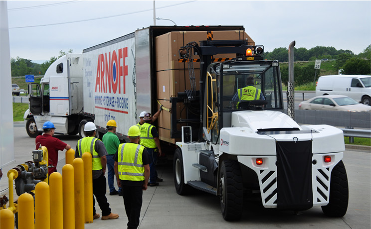
In July of 2013, Nikon announced it had entered into a partnership with SUNY Polytechnic's College of Nanoscale Science and Engineering to develop next generation 450 mm photolithography technology. In April of this year, Governor Andrew M. Cuomo announced installation of the world’s first ever 450 mm immersion scanner had begun at the SUNY Polytechnic Institute's Albany NanoTech Complex.
Toshikazu Umatate, General Manager of the Nikon Corporation Semiconductor Lithography Business Unit said, "Our 450 mm program is advancing well. The NSR-S650D shipped earlier this year as planned, and we will transition to wafer patterning soon. The program's steady progress is a direct result of tireless collaborative efforts across the 450 mm consortium." Umatate added, "Nikon is dedicated to supporting the industry's drive to next generation semiconductor manufacturing through continuous innovations in lithography system performance and productivity."
The information is current as of the date of publication. It is subject to change without notice.