Orders Begin in July for Digital Lithography System DSP-100
Nikon Announces First Back-End Process Lithography System
July 16, 2025
TOKYO - Nikon Corporation will begin accepting orders for the Digital Lithography System DSP-100, designed for back-end semiconductor manufacturing processes, starting in July 2025. This system is specifically developed for advanced packaging applications, supporting large substrates up to 600mm square and delivering high resolution of 1.0μm*1 (L/S*2).
- *11 micrometer (μm) is one-millionth of a meter (one-thousandth of a millimeter).
- *2Abbreviation for Line and Space. Refers to the width of circuit lines and the spacing between adjacent patterns.
Release Overview
| Product name | Digital Lithography System DSP-100 |
|---|---|
| Sales launch | July 2025 |
| Scheduled release | Fiscal Year 2026 |
Development Background
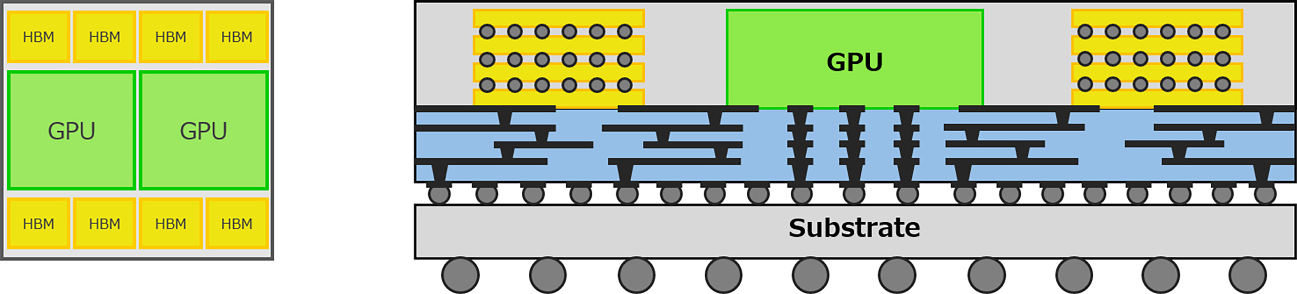
With the widespread adoption of high-speed communication technologies such as the internet of things (IoT) and generative artificial intelligence (AI), the volume of information processing is rapidly increasing, driving demand for high-performance semiconductor devices, especially in data centers. In addition, as advanced packaging technologies such as chiplets - that connect multiple chips side by side - continue to progress, circuit patterns are becoming increasingly fine, and package sizes are growing. In response to these challenges, demand for panel-level packaging (PLP) using resin or glass substrates is expected to see continued growth.
Performance Overview
![]() Swipe horizontally to view full table.
Swipe horizontally to view full table.
| Resolution | 1.0μm L/S |
|---|---|
| Light Source | Equivalent to i-line |
| Overlay Accuracy | ≦±0.3μm |
| Supported Substrate Size*3 | Square substrate: up to 600x600mm |
| Throughput | 50 panels/hour (with 510x515mm substrate) |
- *3Compatible with wafers and even larger substrates
Key Benefits
Combining High Resolution and Productivity
The DSP-100 integrates Nikon's high-resolution semiconductor lithography technology with the multi-lens technology*4 from its flat panel display (FPD) lithography systems. It delivers high resolution (1.0μm L/S), excellent overlay accuracy (≦±0.3μm), and high productivity - up to 50 panels per hour using 510×515mm substrates.
- *4Nikon's proprietary technology exposes multiple projection lenses in an array and precisely controls them to produce the same effect as if a single giant lens were used. This enables patterning over a wider area with a single exposure.
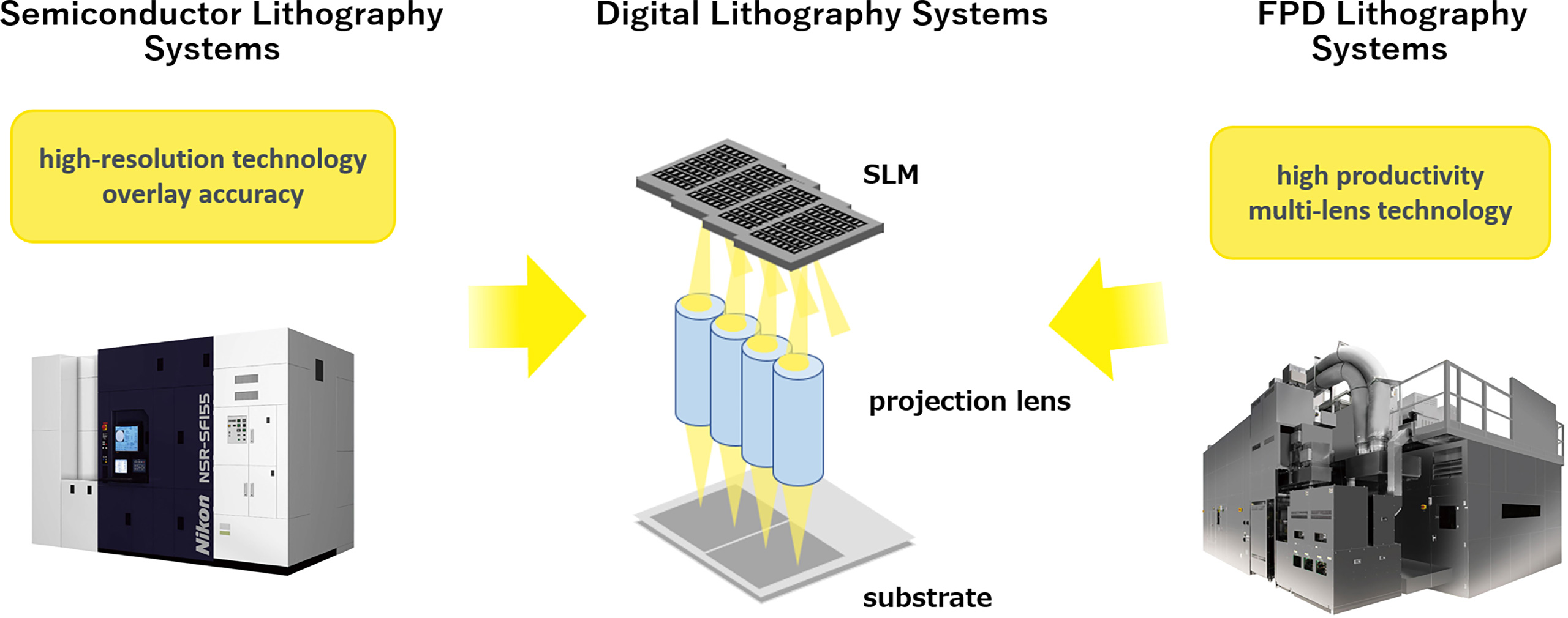
Maskless Operation for Large Advanced Packaging Applications
Unlike conventional lithography systems that require photomasks with circuit patterns, the DSP-100 uses a spatial light modulator (SLM) to directly project circuit patterns onto substrates without the need for a photomask. This approach eliminates the size constraints of photomasks, provides greater flexibility for large, advanced packaging applications, and streamlines the development process - reducing both cost and lead time for customers.
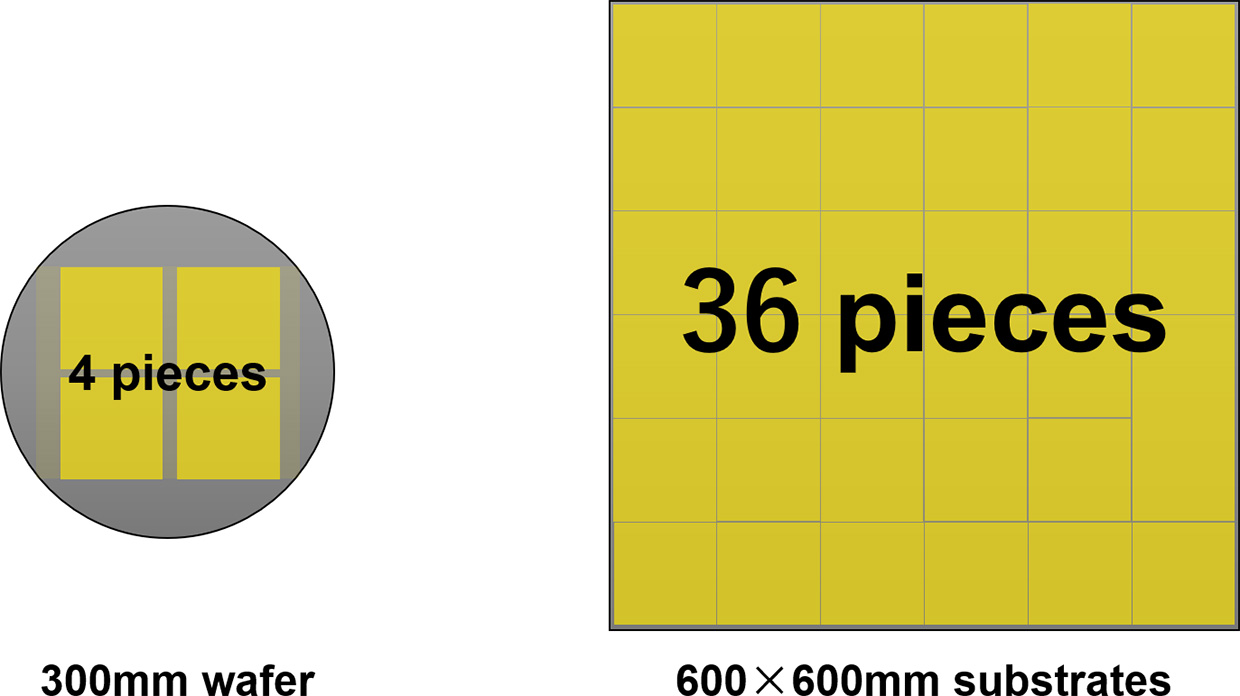
Support for Large Square Substrates - 9x Productivity Compared to Wafers
The DSP-100 supports exposure on large square substrates up to 600×600mm. For 100mm-square large packages, productivity per substrate is nine times higher than when utilizing 300mm wafers. Additionally, the system offers high-precision correction for substrate warpage and deformation, reducing production costs with maskless technology and minimizing maintenance costs with solid state light sources, supporting greener manufacturing.
The information is current as of the date of publication. It is subject to change without notice.