Reusing semiconductor lithography systems to reduce waste
highlight
Nikon conducts initiatives to reuse products and materials, reduce the use of new resources as much as possible, and help realize a resource-circulating society. As part of these efforts, Nikon is promoting the reuse of semiconductor lithography systems to reduce waste.
Shifting from disposal to recycling resources
In the past, society tended to use and then dispose of the waste created by the vast amount of resources it consumed. Today, however, people are cutting down on the waste they generate and reducing new resource consumption by reusing products and materials. Corporations, too, are expected to contribute to these efforts to create a greener society. Accordingly, Nikon has set the goal of realizing a resource-circulating society in its Long-term Environmental Vision and promotes environmental initiatives.

The 3Rs of reducing, recycling and reusing are an integral part of this approach. Nikon proactively engages the 3Rs of (1) reusing products and materials, (2) reducing the amount of waste from manufacturing and sales through innovative solutions and (3) recycling waste materials to be used as resources.
Reselling semiconductor lithography systems and refurbishing their lenses
For almost two decades, Nikon has promoted the reuse of semiconductor lithography equipment to reduce waste.
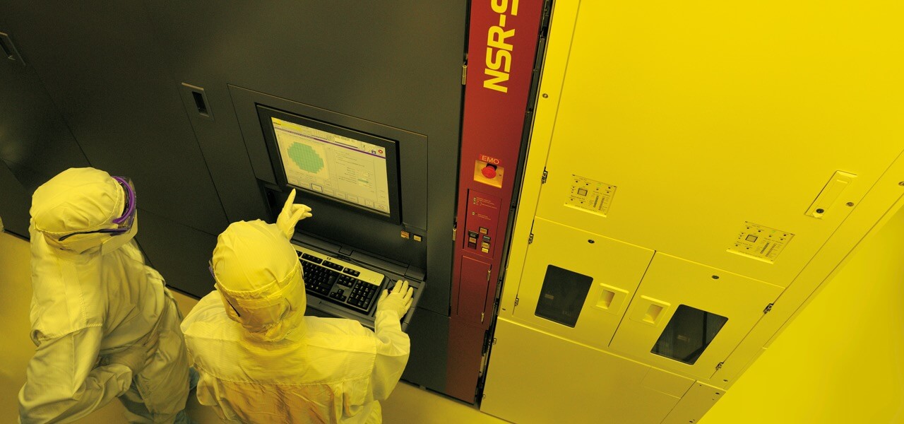
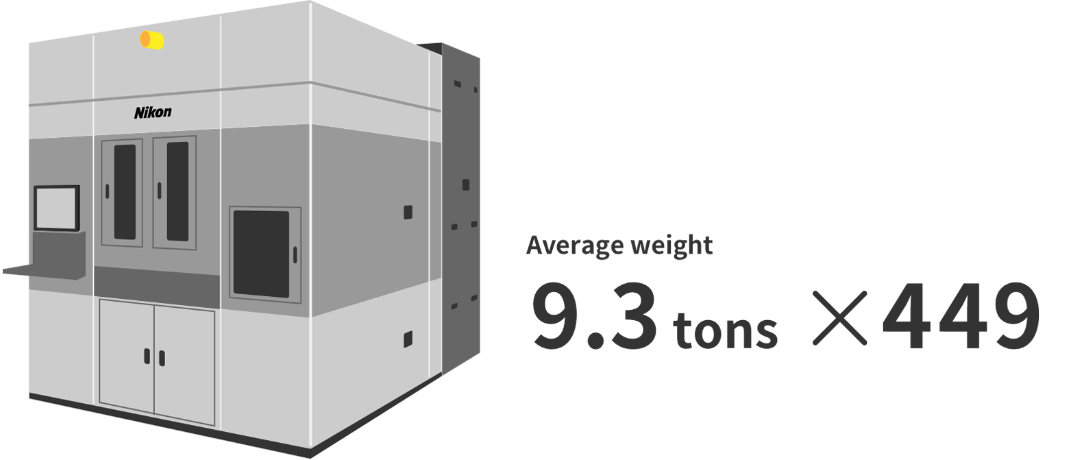
Nikon manufactures the semiconductor lithography systems essential to semiconductor production. After customers finish using these systems, Nikon buys them back, restores their parts and components, and resells them. Nikon launched this business initiative to reuse the systems in 2000 - ahead of its competitors in the industry. By March 2023, 449 systems had been resold, effectively reducing waste materials that would have been disposed of by about 4,100 tons. Lithography systems have grown larger in size with advancements in semiconductor products, so their reuse has become increasingly important for reducing waste materials.
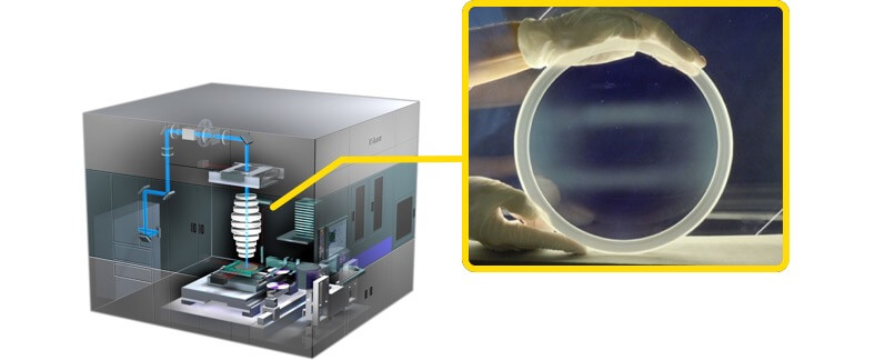
Nikon has also promoted reuse and reduce initiatives for the projection lenses fitted in these lithography systems. While these systems have an operational life of more than 20 years, the projection lenses gradually deteriorate due to ultraviolet rays and other light sources. When they reach the end of their service life, Nikon replaces the entire projection lens unit with a new one. By doing so, Nikon enables lithography systems not only to be used for a longer period, but also reduces waste while realizing higher quality products.
Nikon’s solutions for assembling complete lithography systems from units no longer used
Nikon applies various specialized techniques in its reuse and reduce initiatives.
Lithography systems comprise many separate units, from glass components and mechanical parts to electrical components, exposure devices and air conditioners. If just one of these units deteriorates in quality, the system cannot operate properly. Therefore, Nikon purchases lithography systems that customers no longer use, collects the usable units from numerous lithography systems and assembles them into new systems. It also collects the parts of any remaining units for reuse as replacements.
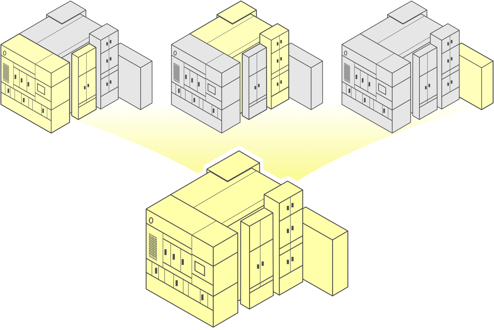
Nikon’s services include exchanging the projection lenses of used lithography systems from customers’ plants and restoring them so they can be used for longer. In the past, this required bringing the entire lithography system to a Nikon’s plant, but Nikon has simplified this process by taking only the lenses to the customers’ facilities and replacing them on-site. This results in less fuel used for transportation and overall energy savings.
All of Nikon’s group companies involved in manufacturing lithography systems are working together to promote these services.
Also, by updating the software, Nikon has improved productivity by about 8% without changing the specifications of the lithography systems themselves. Changing the specifications of the hardware, that is, the actual systems, would emit CO2 and be more likely to pollute the environment during the various processes from parts procurement to manufacturing. By updating the software, rather than the hardware, this results in the lithography systems being able to be used for a longer time at the customer’s facilities.
Other ActivitiesFacilitating longer usage
For the miniaturization and high integration of semiconductors, a finer electronic circuit pattern needs to be exposed. Since the circuit patterns are repeatedly exposed on silicon wafers*, the alignment accuracy is extremely important.
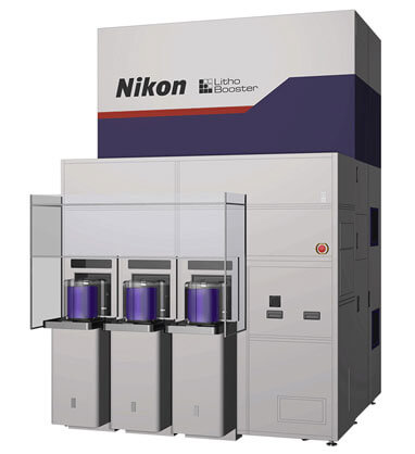
Nikon developed a system that accurately measures and corrects alignment distortion by utilizing its own unique technology that has been cultivated over time. This process is not only integrated into the system in the latest lithography systems, but also commercialized as a standalone alignment station known as the “Litho Booster”.
Adding the Litho Booster to the production line enables higher accuracy overlay and improves the yield during manufacturing. Therefore, customers can utilize the existing lithography systems longer, while simultaneously reducing energy and other waste. Through these means, Nikon is also contributing to the promotion of the 3Rs for customers, taking advantage of its advanced technological capabilities.
- *In semiconductor manufacturing, highly complex circuit patterns printed on a photomask made of a glass plate are reduced in size using ultra-high-performance lenses and exposed onto a silicon substrate known as a wafer. When the electronic circuit patterns are repeatedly exposed onto the silicon wafer, they are positioned at a nanometer level of accuracy employing Nikon technology.
OutlookOngoing initiatives to realize a resource-circulating society

In semiconductor manufacturing, models 10 to 20 years old are still viable. Nikon is able to respond to various needs for lithography systems not only through maintenance but also by promoting the 3Rs - thanks to its advanced technologies cultivated over the years. At the same time, Nikon continues to pass on these technologies to new generations, thereby strengthening human resources. It can be said that advanced technology and the dissemination of knowledge and know-how to new generations are greatly supporting Nikon in this day and age.
Along with its efforts to reuse semiconductor lithography systems and reduce waste, Nikon aims to recycle resources in all of its products. Measures for saving resources and reducing waste are carried out during all processes, from product development and design through to production and sales. The entire Nikon Group is committed to realizing a resource-circulating society.
Related SDGs
SDGs: Sustainable Development Goals
In 2015, the international community adopted a set of targets for sustainable development, to be achieved by 2030. The 17 global goals address issues such as poverty, hunger, education and climate change.
Related information
Brand Movie 「Environment」
Explore Nikon's environmental initiatives. (02:34)
Highlight
- The Power of Imaging: Bridging Space and Earth
- Riblet Processing — A Technological Innovation for Aircraft Leading Toward Achieving Carbon Neutrality
- Reusing semiconductor lithography systems to reduce waste
- Supporting children’s education in Laos
- Providing solutions for iPS cell-based drug discovery
- Reducing CO2 emissions from lens manufacturing process through technology
- Product Manufacturing and Social Contributions through Sharing Our Vision with Procurement Partners
- Fostering “Image Culture” through the Nikon Photo Contest A Conversation with those Inspired by Photography
- Worldwide employee training: ensuring Nikon remains a company that people trust
- Superior quality born from a collaborative production process