Development of a stacked CMOS image sensor
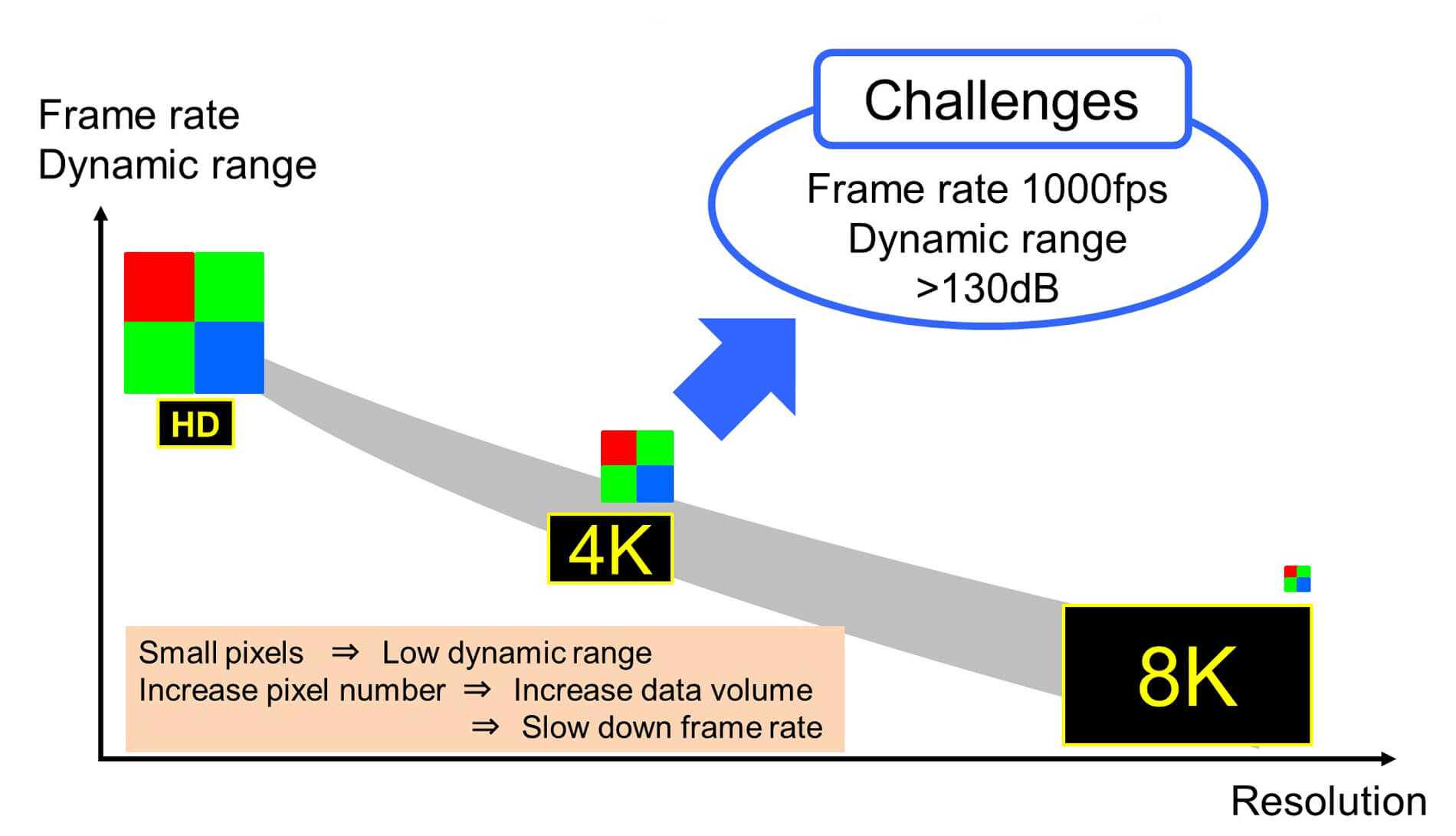
High-speed, high-resolution, wide-dynamic-range imaging
March 3, 2021
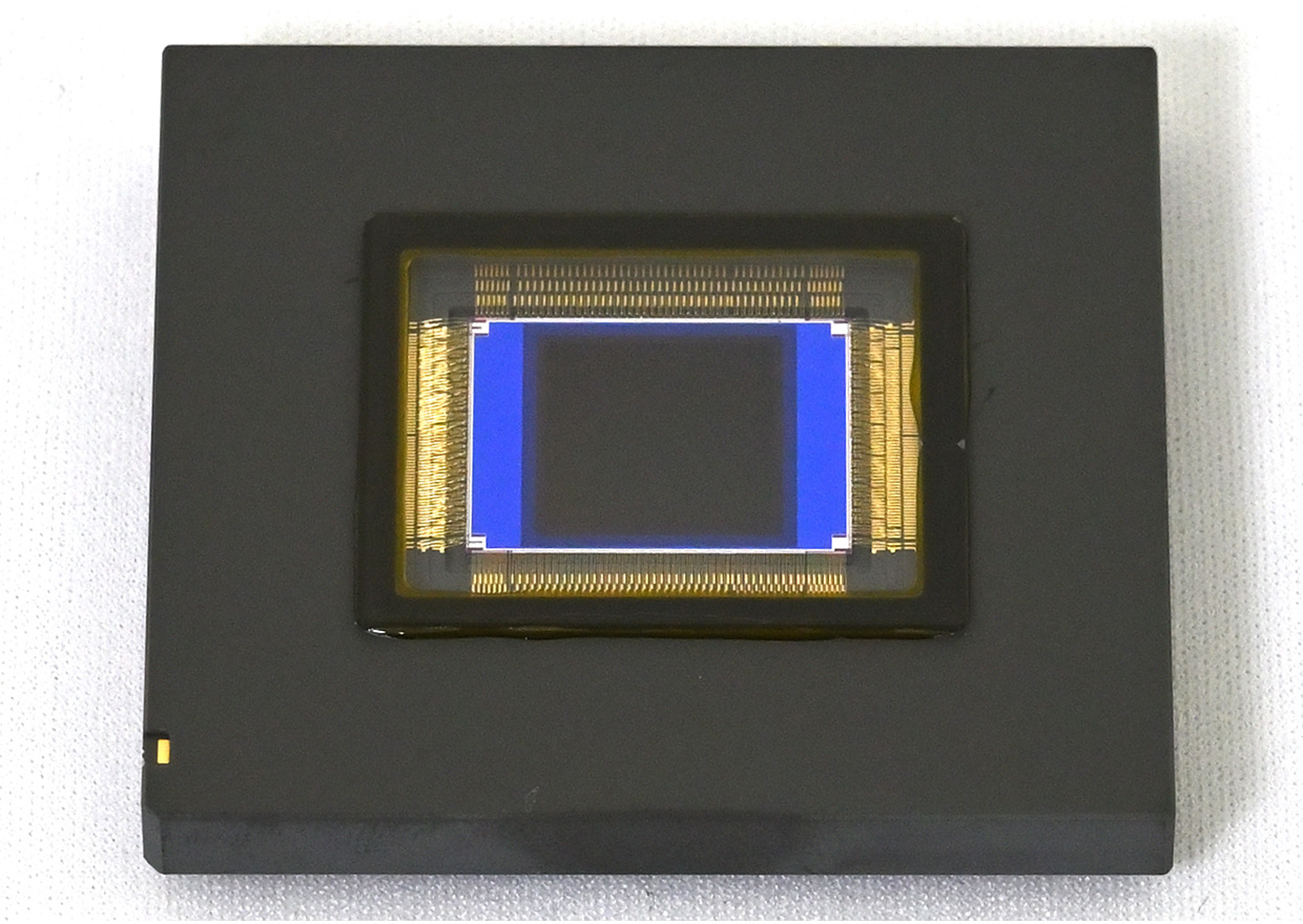
TOKYO - Nikon Corporation (Nikon) has developed a stacked, 4K × 4K, CMOS image sensor with a total pixel count of approximately 17.8 megapixels that realizes high-resolution imaging with 1000 frames per second, and high dynamic range (HDR) characteristics of 110 dB.
This result was announced at the ISSCC (International Solid-State Circuits Conference) held in San Francisco, USA from February 15, 2021.
Development background
As an optical instrument manufacturer, Nikon is also engaged in research and development of cutting-edge image sensor technology. These efforts build upon Nikon's optical technology, precision measurement / manufacturing technology, and material technology. Currently, image sensors are used not only in imaging field with digital cameras and smartphones, but also in various industrial fields such as automotive. In all fields, there is a demand for image sensors that realize the full combination of compactness, light weight, high frame rate, wide dynamic range, and high resolution.
Image sensor technology development is indispensable for Nikon, and we will continue to research and develop sensors in response to market demands.
Main features
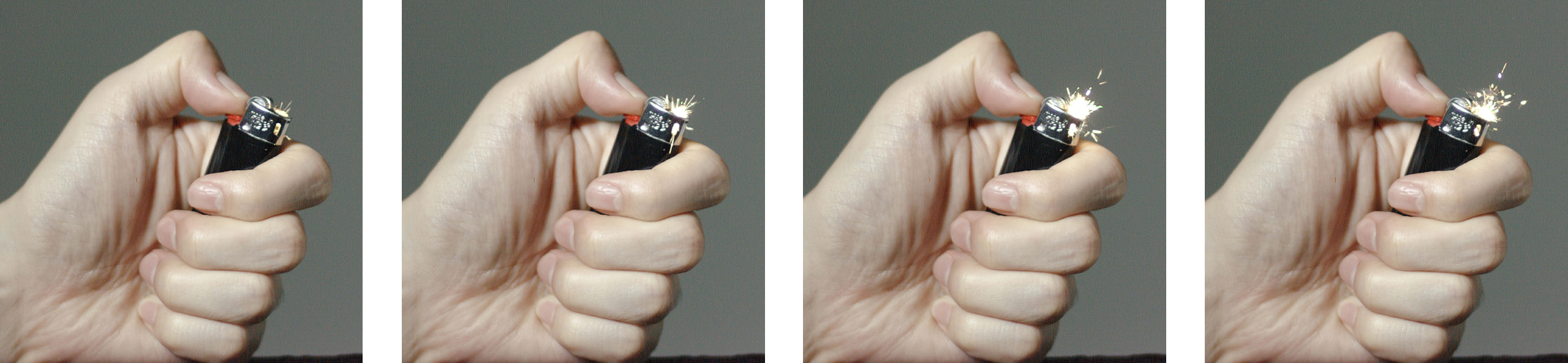
1. Most advanced level of HDR characteristics of 110 dB and high-speed shooting of 1000 frames per second*
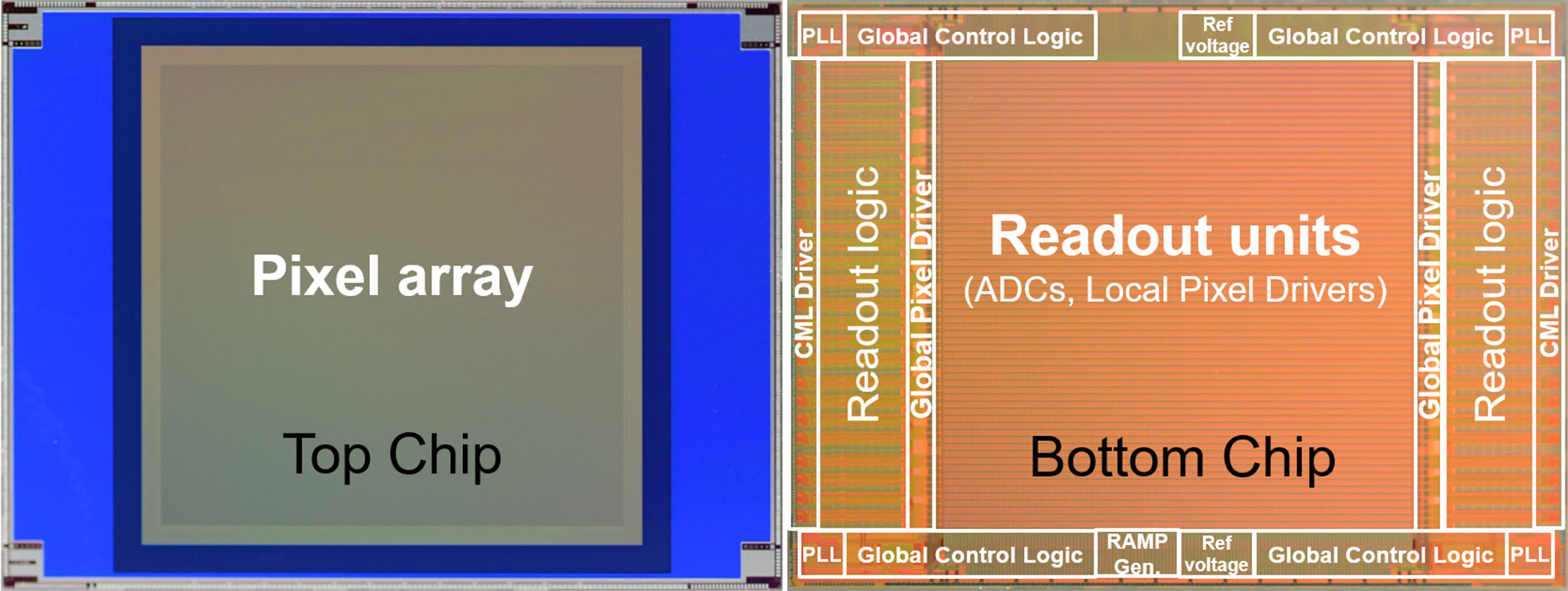
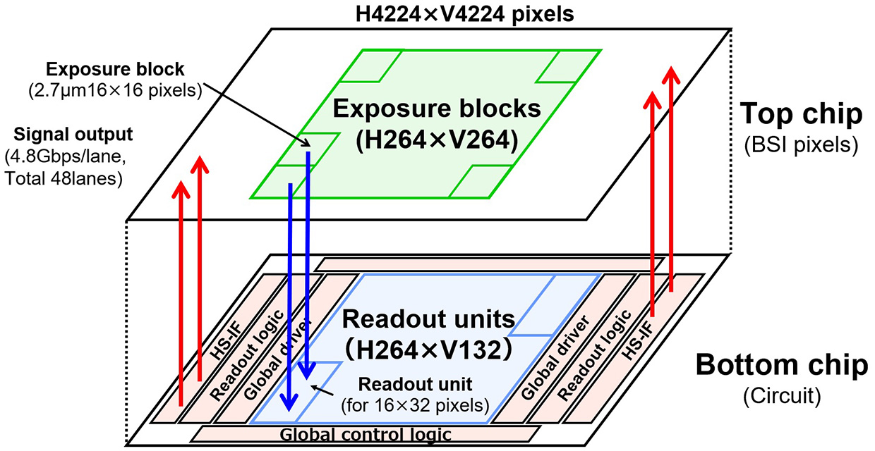
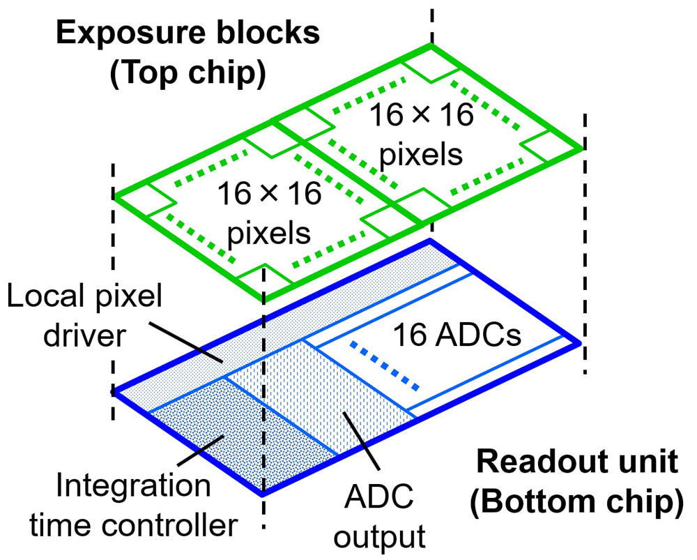
This sensor uses a fine-pitch wafer level wire connection technology consistent with the 2.7 μm pixel size. This makes it possible to control the top chip with the image sensor directly from the logic circuit of the bottom chip. It has a high resolution of 4K × 4K pixels, a wide dynamic range of 110 dB, and high-speed shooting of 1000 frames per second. High-speed readout enables super slow motion shooting of up to 1000 frames per second.
It also has a wide dynamic range of 134 dB for shooting 60 frames per second.
- *2.7 μm pixel size or less. As of February 15, 2021, according to Nikon research.
2. Exposure can be controlled for each area on the sensor
The top chip is divided into individual blocks of 16 × 16 pixels, with a total of 264 × 264 blocks (4224 × 4224 pixels) arranged on the sensor. Exposure in each area of the image can be tuned by finely controlling the exposure time of each of the blocks. This is achieved using the bottom chip control architecture.
With this function, users can experience a wide dynamic range, even for subjects with large differences in brightness. Users can clearly shoot the entire scene without crushing the dark areas or overexposing the bright areas.

The wide dynamic range enables both dark and bright areas to be imaged with single shot.
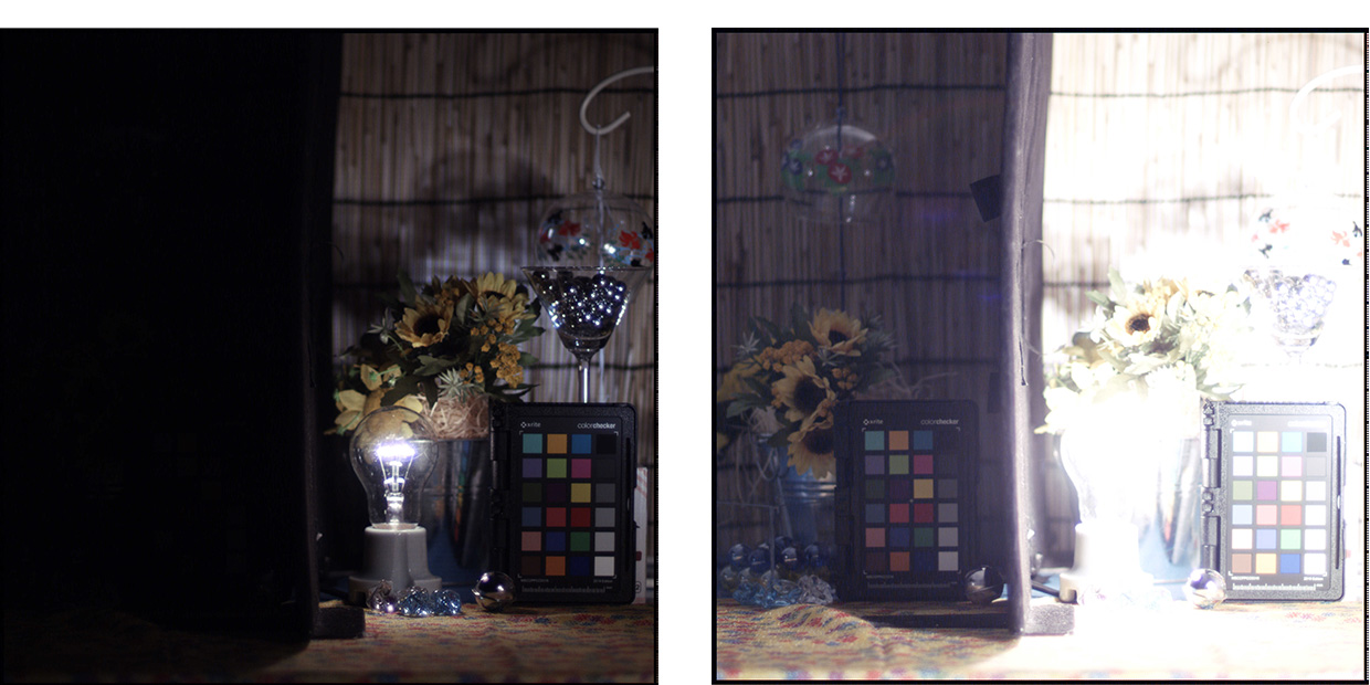
Image on the left: Adjusted to the bright part.
Image on the right: Adjusted to the dark part.
Main Specifications
![]() Swipe horizontally to view full table.
Swipe horizontally to view full table.
| Manufacturing process | 65 nm BSI + 65 nm CMOS Wafer level stacking process |
|---|---|
| Image sensor | 1-inch CMOS image sensor |
| Pixel size | 2.7 × 2.7 μm |
| Frame rate | 1000 fps |
| Dynamic range | 110 dB (at 1000 fps) 134 dB (at 60 fps) |
| Total number of pixels | Approximately 17.8 megapixels (4224 × 4224 pixels) |
The information is current as of the date of publication. It is subject to change without notice.