Nikon Releases New NSR-S625E ArF immersion scanner
Highest Productivity in the History of Nikon Lithography Systems
May 8, 2023
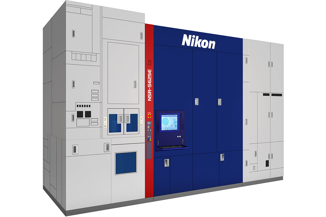
TOKYO - Nikon Corporation is pleased to announce the release of the NSR-S625E, an ArF immersion scanner optimized especially for middle critical layers. The NSR-S625E, with the highest productivity in the history of Nikon's lithography systems thanks to its enhanced throughput and operational stability, will contribute to efficient production of various semiconductor devices.
Product name and release data
| Product name | NSR-S625E ArF immersion scanner |
|---|---|
| Sales launch | February, 2024 |
Development background
The semiconductor devices demanded vary widely along with the diversification of their applications. Requirement for lithography systems, which are essential for semiconductor device manufacturing, is becoming more complex and sophisticated. Nikon has been providing best solutions while pursuing companionship with its customers. To satisfy the diverse customer needs more than before and to expand its product lineup, Nikon has developed a new lithography system. The NSR-S625E, the newly developed system, is the successor to the NSR-S622D, which boasts a 10-year sales period. The NSR-S625E, with a throughput approximately 1.3 times that of the NSR-S622D, significantly improved operational stability, and an iAS*1 incorporated, contributes to enhanced production efficiency for a wide range of semiconductor devices.
Nikon will continue to contribute to the manufacturing of high-value-added semiconductor devices by providing lithography systems that best suit customer needs.
- *1inline Alignment Station: The alignment station performs high-speed, ultra-precise measurement of all wafers, and then corrects problematic grid errors without reducing the throughput of the lithography system.
Performance Overview
![]() Swipe horizontally to view full table.
Swipe horizontally to view full table.
| Resolution | ≦ 38 nm |
|---|---|
| NA | 1.35 |
| Exposure light source | ArF excimer laser (193 nm wavelength) |
| Reduction ratio | 1:4 |
| Maximum exposure field | 26 mm x 33 mm |
| Overlay | SMO*1:≦ 1.7 nm, MMO*2:≦ 2.5 nm |
| Throughput | ≧ 280 wafers/hour (96 shots) |
- *1Single Machine Overlay: machine-to-self overlay accuracy (NSR-S625E #1 to NSR-S625E #1)
- *2Mix and Match Overlay: machine-to-machine overlay accuracy (NSR-S625E #1 to NSR-S625E #2)
The information is current as of the date of publication. It is subject to change without notice.