Development of a 1.5 µm Resolution Digital Lithography System
Nikon Expands Digital Lithography Lineup for Advanced Packaging
June 5, 2026
TOKYO - Nikon Corporation is developing a high-productivity digital lithography system for advanced packaging processes in semiconductor manufacturing back-end operations. The system delivers resolution of 1.5 µm*1 (L/S) *2 and is designed to further enhance productivity.
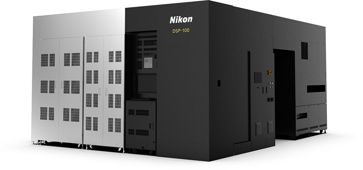
Throughput is targeted to improve by more than 30 %, from 50 panels per hour achieved by the DSP-100 digital lithography system*3 to 65 panels per hour or higher*4. The new system is scheduled for release in fiscal year 2027.
Development Background
Demand for next generation semiconductor devices, including GPUs and high-bandwidth memory (HBM), continues to expand with the growth of generative AI. Adoption of advanced packaging technologies that interconnect multiple semiconductor chips is accelerating.
Panel level packaging is gaining traction as manufacturers seek higher productivity. At the same time, wiring requirements for large interposers and FC-BGA substrates used to connect multiple chips are becoming more diverse, depending on customer processes. Required resolution varies across applications.
To address these evolving needs identified through close collaboration with customers, Nikon is expanding its digital lithography system lineup.
In addition to the DSP-100, which offers 1.0 µm (L/S) resolution, Nikon is developing a new system equipped with optics optimized for 1.5 µm (L/S) resolution. This enables higher productivity while supporting a broader range of process requirements.
Flexible Configuration for Future Needs
The new system is designed with flexibility in mind. By exchanging the optical system, it can support 1.0 µm (L/S) resolution, equivalent to the DSP-100, allowing customers to adapt to future process requirements while supporting long term use.
Key Features
Enhanced Productivity While Leveraging Proven Performance
Building on Nikon's digital lithography platform, the new system is designed to deliver higher throughput, targeting 65 panels per hour or more, while maintaining the strong performance foundation established by the DSP-100, which already achieves 50 panels per hour.
Maskless Architecture for Greater Efficiency
As with Nikon's digital lithography systems, the new platform eliminates the need for photomasks. This contributes to reduced costs and shorter development and production cycles for customers.
Combination of High Resolution and High Productivity
Nikon combines its semiconductor lithography expertise in high-resolution imaging with the high-productivity capabilities cultivated through FPD lithography systems. Backed by extensive experience in both fields and a robust support infrastructure, Nikon continues to deliver reliable solutions to customers.
Commitment to Customer Value
Nikon will continue to meet diverse customer needs by providing optimal lithography solutions, contributing to higher-value semiconductor manufacturing.
- One micrometer (µm) equals one-millionth of a meter (one-thousandth of a millimeter).
- L/S (Line and Space) refers to the width of circuit lines and the spacing between adjacent patterns.
- The DSP-100 is a digital lithography system scheduled for release in fiscal year 2026 (orders began July 2025).
https://www.nikon.com/company/news/2025/0716_01.html - Based on 510 × 515 mm substrates.
- FC-BGA stands for Flip Chip Ball Grid Array, a high-density semiconductor package substrate enabling higher performance and functionality in LSI chips.
The information is current as of the date of publication. It is subject to change without notice.