Manufacturing glass that grows like a lifeform

Synthetic quartz glass: essential for semiconductor lithography systems
Semiconductors support the evolution of IoT and AI and are indispensable
for developing the society of the future.
Nikon's semiconductor lithography systems greatly contribute
to the quality of these essential semiconductors.
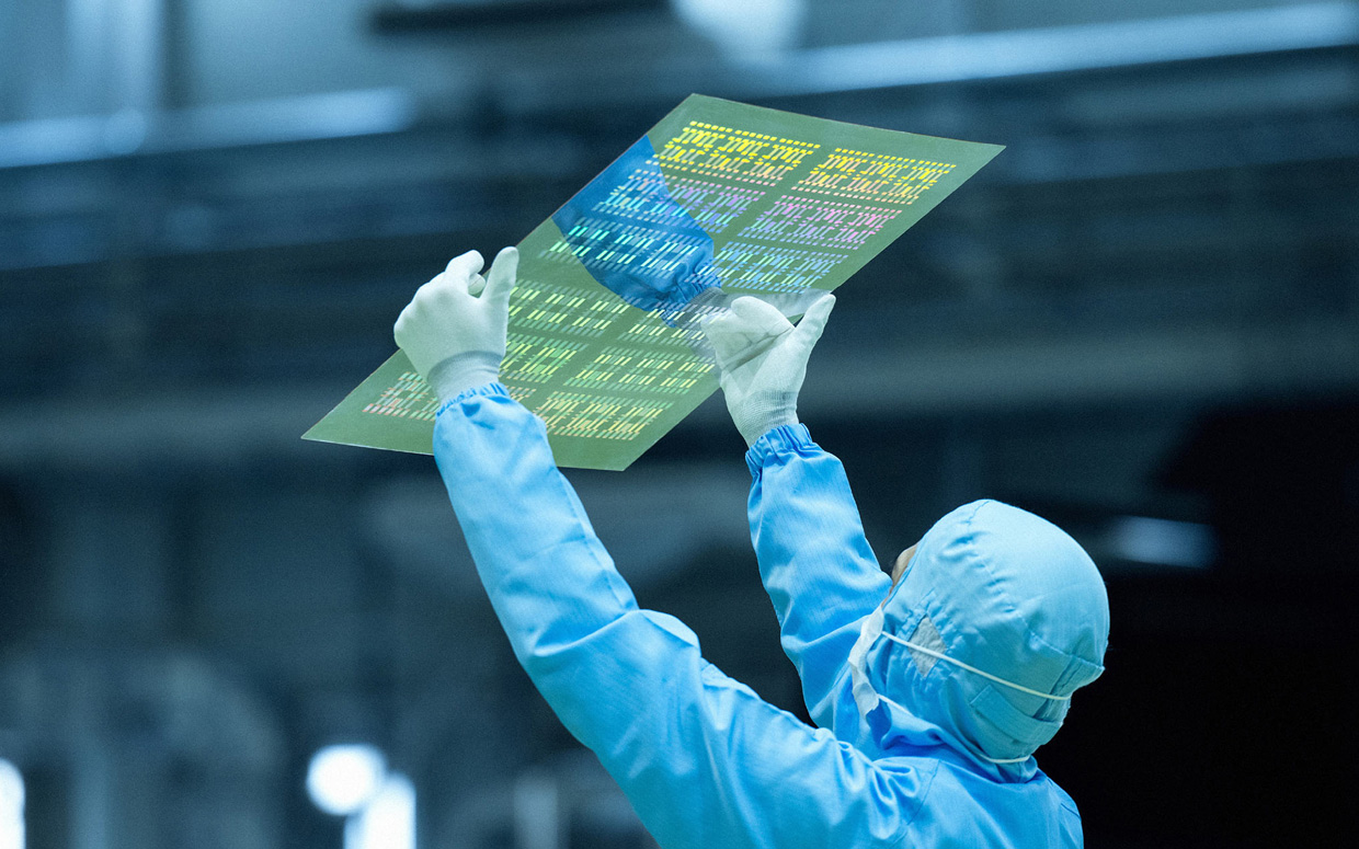
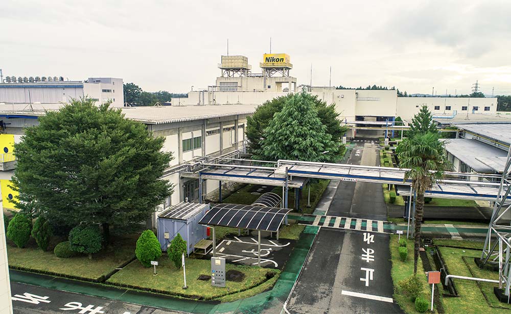
The key lenses employed in these systems are made of synthetic silica glass that achieves outstanding optical performance, manufactured at Nikon's Sagamihara plant.
Thermal stability and optical transmittance for advanced patterning
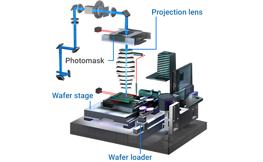
Semiconductor lithography systems use a projection lens to reduce semiconductor electric circuit patterns drawn on a large glass plate (photomask), and then expose them onto a semiconductor material (silicon wafer).
High-performance semiconductor circuit patterns are exposed with short-wavelength UV* light. In order to transmit such light, the lens must be extremely transparent. In addition, since light heats the lens, it is essential that form and characteristics changes caused by heat must be minimal.
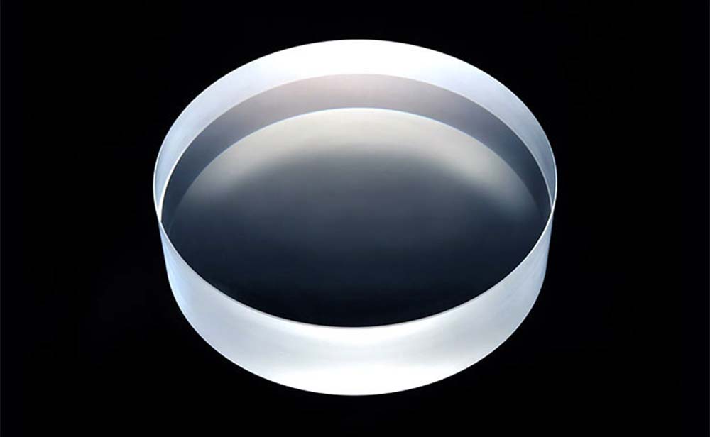
In order to manufacture such lenses, particularly high-quality materials are required. This is synthetic silica glass.
The most distinctive feature of synthetic silica glass is that it is almost entirely made of silicon dioxide (SiO2). Because of very few impurities, the transparency is extremely high and the glass suffers almost no deformation due to heat.
So why does synthetic silica glass contain fewer impurities than ordinary glass? The reason lies in the meticulous manufacturing method.
- *KrF Excimer laser (wavelength: 248 nanometers) or an ArF Excimer laser (wavelength: 193 nanometers).
A nanometer is equal to one billionth of a meter.
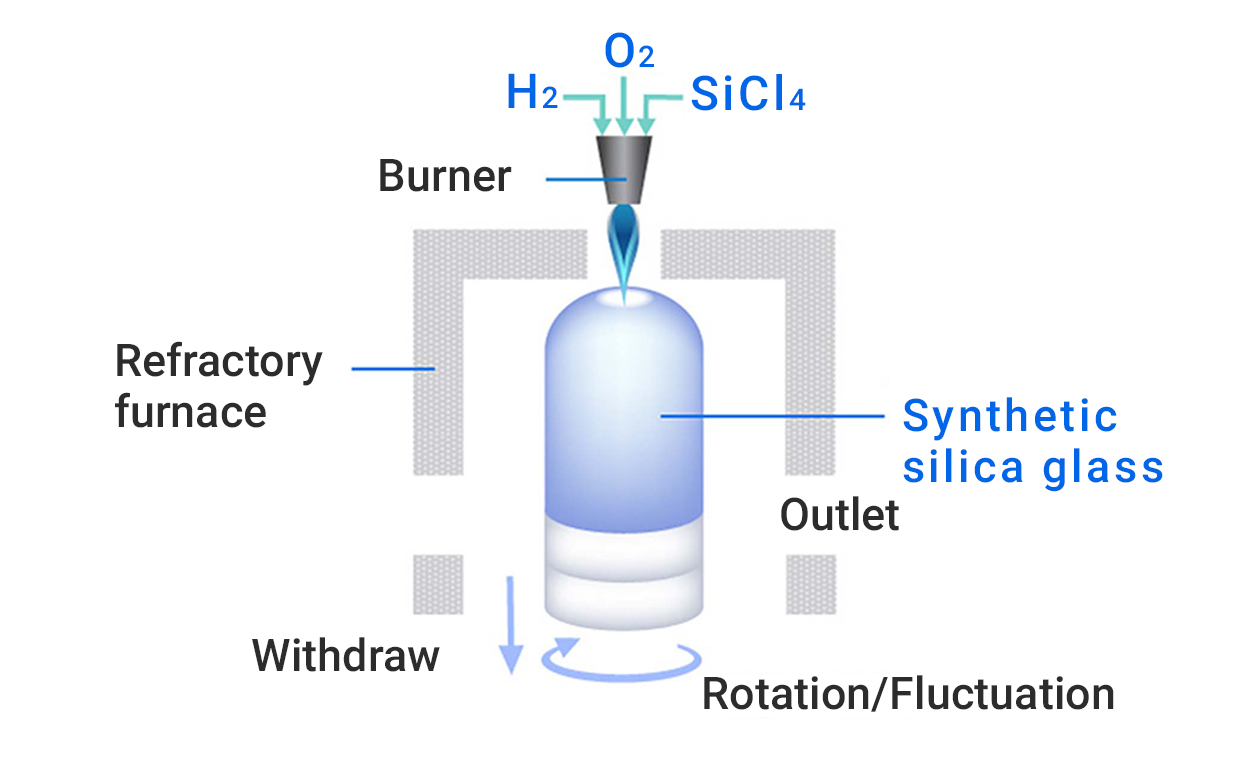
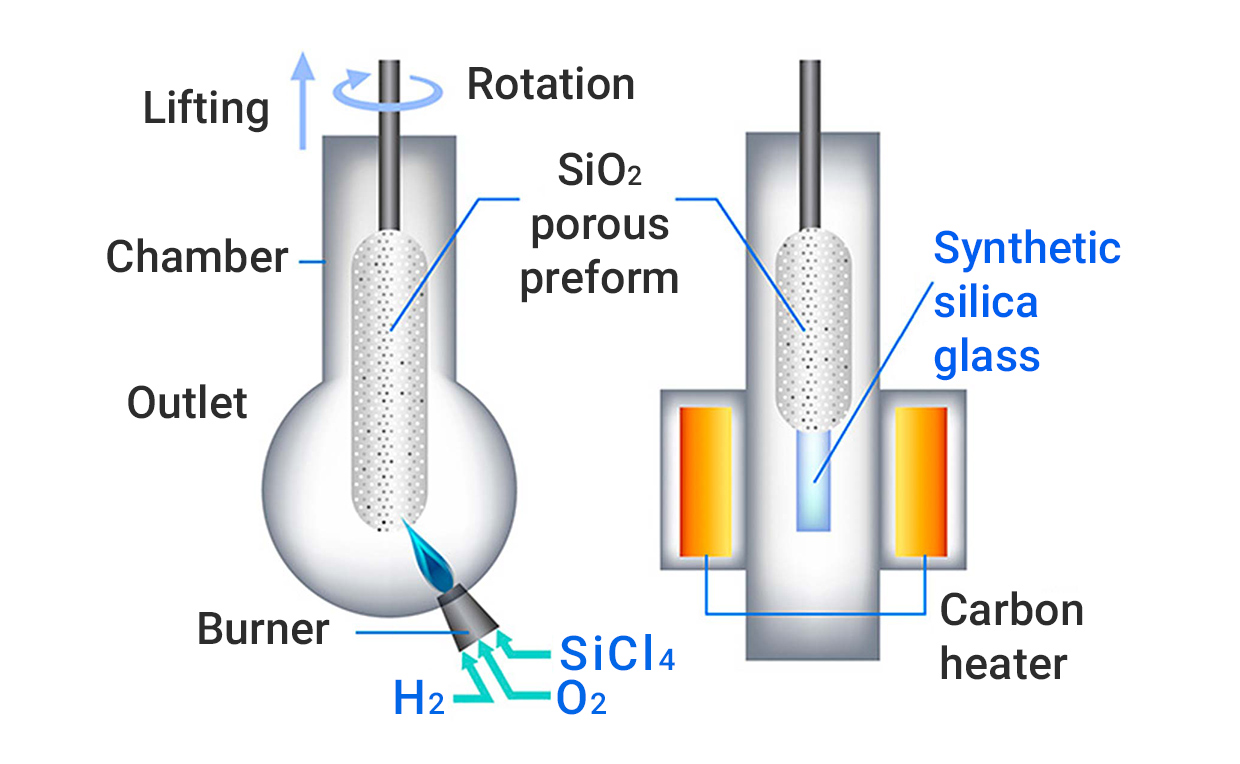
Ingot production methods: Direct and Soot methods
Nikon utilizes two major methods of manufacturing synthetic silica glass.
One of these is the direct method (Figure 1). It consists of causing vaporized material (silicon tetrachloride/SiCl4) to react with oxygen and hydrogen to form silica glass particles which are then deposited from above so that a large block can be manufactured.
Water and hydrochloric acid produced during the reaction are vented out of the furnace. Since the silica glass particles do not touch the walls of the furnace, there is almost no contamination with impurities.
The other method is the soot method (Figure 2). The materials employed are the same, but the glass is created through two processes: synthesis and sintering. The synthesis is almost the same as the direct method. However, due to a low reaction temperature, the silica glass is deposited with gaps between the particles. Therefore, it moves on to a sintering process that removes water generated from hydroxyl groups on the particle surfaces. Since this method can further reduce water that would otherwise become an impurity it enables a silica glass of higher purity to be produced.
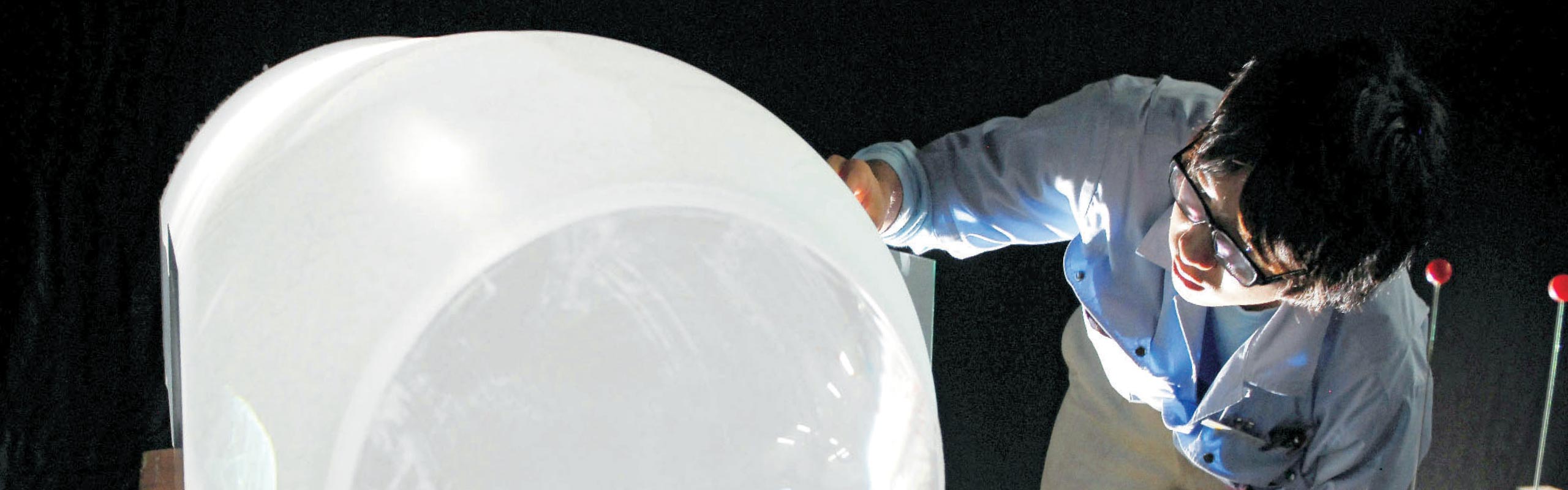
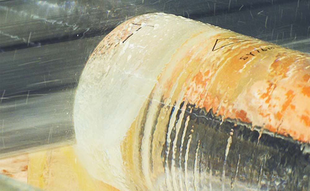
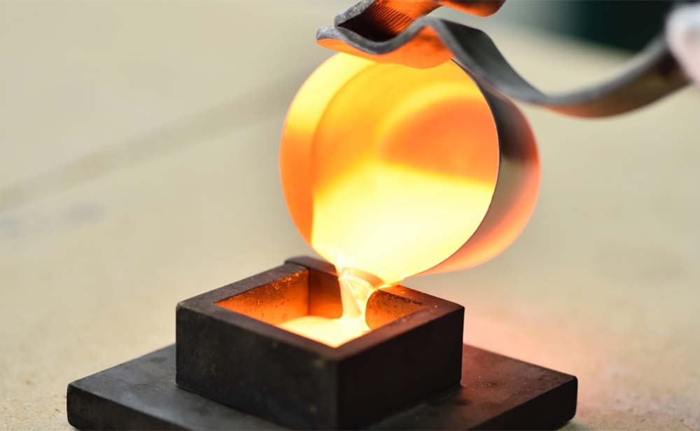
Both manufacturing methods result in cylindrical ingots (masses of synthetic silica glass). Ingots manufactured by the direct method may weigh several hundreds of kilograms.
How an ingot is prepared before shipping as lens materials
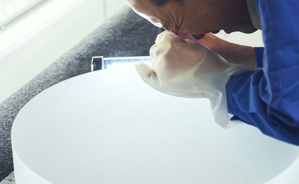
After shaving both sides of an ingot, its interior condition is checked by individual inspection, cut to the required thickness avoiding any flaws and the outer periphery is shaved (rounding). At this stage, the inside structure of an ingot is not stable. Therefore, it is reheated in an annealing furnace and then cooled slowly to stabilize its structure. After this, the synthetic silica glass is inspected again and transferred to each lens manufacturing plant.


Commitment to quality
Nikon's manufacturing attitude of never compromising quality is of course consistently applied to the production of synthetic silica glass. The most important part of synthetic silica glass production is the synthesis process. Since properties of the furnaces differ, the glass being synthesized is measured piece by piece, and the data is fed back to technicians. While trying to manufacture it under the best conditions, the direct method takes about one month to "grow" the ingot in the furnace. Also, engineers and on-site specialists who are most familiar with the furnaces' properties work closely together. This unhindered sharing of information between both parties enables manufacturing for various different purposes to be successful.
Also, having a wide variety of high-precision evaluators, Nikon utilizes measurement data in the development and manufacturing to support optical quality improvement.
Synthetic silica glass is formed into a large ingot taking the greatest care. In the future, Nikon hopes to improve its technology for manufacturing glass with targeted characteristics and to expand its applications to products other than semiconductor lithography systems.
Advancing technology development for a wider range for applications

Production Technology Division
Aya Hirai
My role is serving as a general hub involving many exchanges with other divisions regarding processing and inspection, in addition to manufacturing. When I was first involved in the creation of synthetic silica glass, I was really looking forward to enlarging ingots. Now I really feel rewarded to know that the manufacturing of new specification glass is on track, and to be complimented by my colleagues in the business unit when I find myself immediately handling any errors in the previous processes.
There are still many fields in which silica glass should be used instead of ordinary optical glass. We will advance our technology development including cost matters to fully meet expectations, so that this glass can be successfully used in optical components and modules.

Production Technology Division
Takuichi Saito
I have been involved in synthesis technology since starting work with Nikon, but now I believe that my job is to act as a bridge between the manufacturing site and engineers. I try to quantify what people at the site are saying as intuitively as possible, simplify the technical terms used by engineers, translate these words and deliver the intent of both parties, which is both interesting and difficult.
During manufacturing, there are some procedures that require fine-tuned craftsmanship. I'd like to organize such processes logically and create a common language. My goal is to run the PDCA cycle even without involving engineers, which would increase productivity and reduce costs, so it could be used for a wider range of applications.
- *Division and responsibilities are as of the time of the interviews.
Stories "Advancing Monodzukuri (manufacturing) through synergetic innovation"
Most of Nikon's synthetic silica glass is used in projection lenses for semiconductor lithography systems at Tochigi Nikon. Learn about advanced manufacturing at this facility handling production of optical components.
Synthetic Silica Glass Product Website
Nikon provides synthetic silica glass with superior optical properties for diverse applications.
Sustainability Highlight "Reducing CO2 emissions from lens manufacturing process through technology"
Understand Nikon's lens manufacturing operations via the broad range of initiatives and measures that reduce any impact on the environment.
Originally published: April 20, 2020.